Chapter 2: Operational Amplifiers
Table of Contents
- Chapter 2: Operational Amplifiers
Operational amplifiers (op-amps for short) are essential building blocks of modern electronic circuitry. They have a few simple properties. These are:
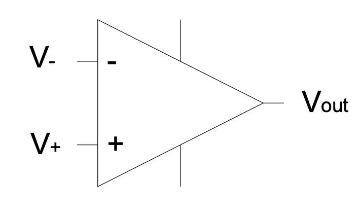 Figure 2.1: Op-amp schematic
’-‘ input: inverting input
’+’ input: non-inverting input
$V_{out}=A_v(V_+-V_-)$ — the fundamental op-amp equation
The other pins are connected to the supply rails.
$A_v$ is called the “open loop gain” of the op-amp. Typically $A_v$ Is between 100 000 and 1 000 000.
In practice $V_{out}$ is limited by the supply voltages to the op-amp.
Ideally no current flows into either of the inputs but in reality this is not exactly the case and will be discussed later.
From the above equation:
- If $V_+ > V_-$: $V_{out}$ goes as high as it can (limited by the positive supply voltage), unless $(V_+ - V_-)$ is on the order of microvolts due to the very high gain.
- If $V_- > V_+$: $V_{out}$ goes as low as it can (limited by the negative supply voltage), unless $(V_- - V_+)$ is on the order of microvolts due to the very high gain.
Negative feedback
A buffer is an example of negative feedback:
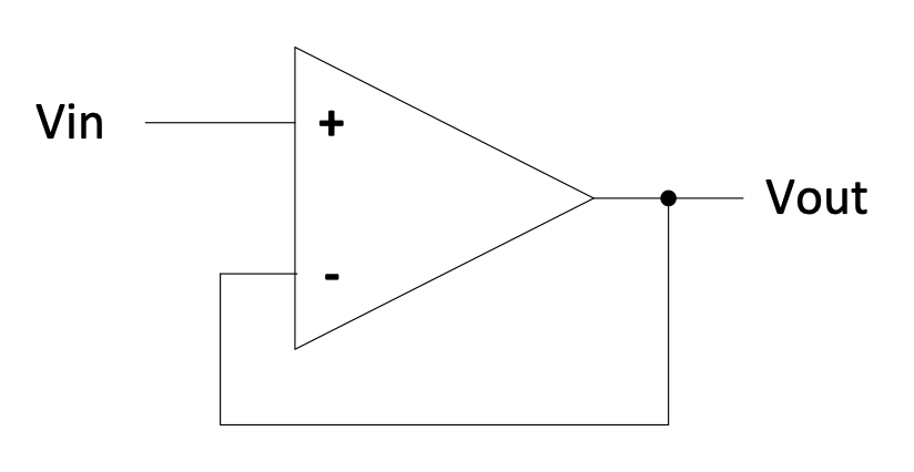 Figure 2.2: Buffer circuit
The inverting and non-inverting amplifiers discussed further on, are also examples of negative feedback.
If we arrange our circuit so that $V_{out}$ affects $V_-$ such that when $V_{out}$ increases so does $V_-$, then we find that the output counteracts itself: The bigger $V_{out}$, the bigger $V_-$, causing $V_{out}$ to decrease. This is called negative feedback.
In practice, if a negative feedback loop exists then the inputs of the op-amp will be driven extremely close to equality, which then satisfies the op-amp equation, provided that the output is not saturated (driven to its extremes). In other words $V_{+}= V_{-}$ because $A_{v}$ is very large. This can directly be seen for the circuit above because $(V_+-V_-)\times A_v=V_{out}$ and $V_{out}$ is given to be not up to its limits. This can only be true with $A_{v}$ very big when $V_+-V_-$ is very small, thus $V_+$ must be about equal to $V_-$ .
Example 2.1
For example, if $V_{in}=10.0$ V, and $A_v=100000$ then the following will be the outcome:
- $V_{out}=10.0\times {100000}/{(1+100000)}=9.9999$ V
(This follows from the equation $V_{out}=(V_{in}-V_{out})\times A_v => V_{out}=V_{in}\frac{A_v}{1+A_v}$)
- $V_+-V_-=V_{in}-V_{out}=0.0001$ V
(If it bothers you that 10.0 – 9.9999 = 0.0001, and 0.0001 x 100 000 = 10.0 which is not equal to 9.9999; this inconsistency is simply because the calculations above are not done to infinite accuracy. The precise answers would have been:
-
$V_{out}=10.0\times {100\ 000}/{(1+100\ 000)}=9.99990000099999000009999900000999990\dots \ V$
-
$V_+-V_-=V_{in}-V_{out}=0.00009999900000999990000099999000009\dots \ V$
In most cases, it will be good enough to simply work with $V_-=V_+$ in the case of negative feedback, therefore $V_{out}=V_{in}=$ 10.0 V in this example.
Another property of the ideal op-amp is that the inputs draw no current, implying that a real op-amp has very high input impedances.
The ideal op-amp has zero output impedance, implying a very low output impedance for a real op-amp.
These rules allow us to analyse just about any op-amp circuit.
The last circuit above is called a buffer or a voltage follower.
It is used to change a high impedance point to a low impedance output, for example when a regulated voltage is required. Anyone of the following circuits will do this:
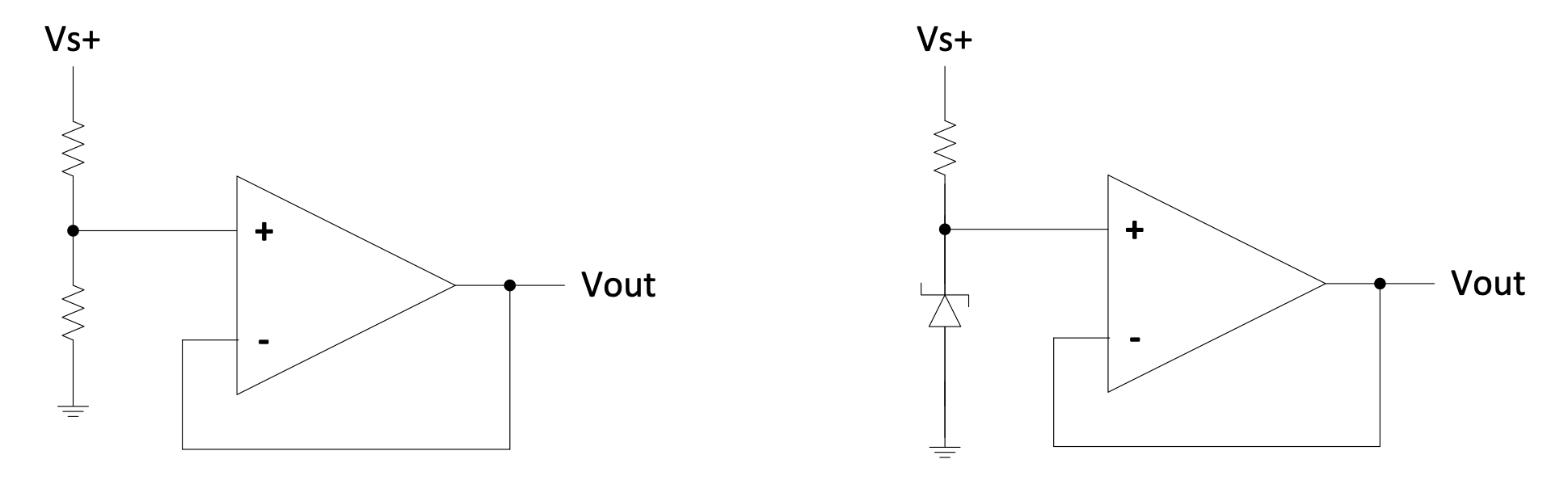 Figure 2.3: Buffer or voltage follower circuit
In the first example the ratio of the resistors will determine the regulated voltage.
In the second example the voltage of the Zener diode will determine the regulated voltage provided that $V_{s+}$ (the positive supply voltage to the op-amp) is higher than the Zener voltage. The resistor must be chosen that the current through the Zener is adequate – typically in the order of 10 mA (but always check the datasheet for your component).
Why is the point connected to the non-inverting input a high impedance point while the output of the op-amp is low impedance? The difference lies in what will happen with the voltage of a point when a load is connected to it. If you connect a load of even relatively high resistance to the non-inverting input in these cases, the voltage there will change. The output of the op-amp is designed to have small impedance – it is actually a small amplifier sitting there. So if you connect a load to the output of the op-amp, the voltage will change only a little bit.
When there is only one feedback from the output to the op-amp inputs, it must be to the –input. If there are feedbacks to both the –input and the +input, the feedback to the –input must be “dominant”. If not, it will be positive feedback and the circuitry will simply drive the op-amp signals to the supply rails.
For example, this is wrong:
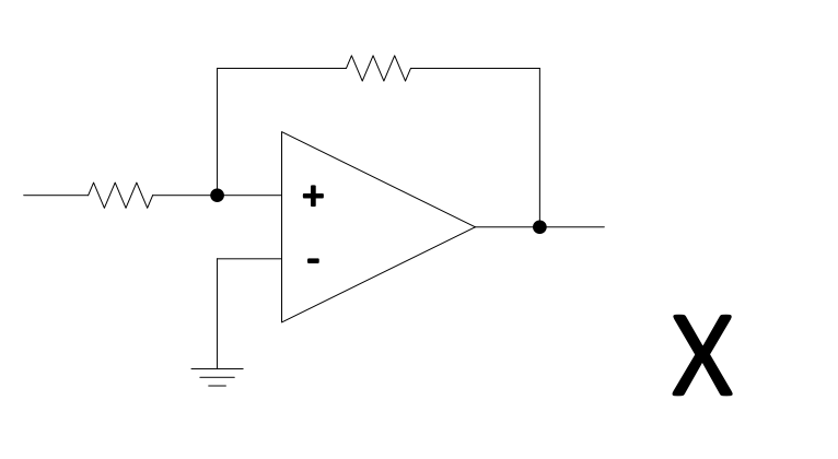 Figure 2.13: Incorrect op-amp network — the feedback to the non-inverting input dominates, causing positive feedback which drives the output to saturation at the supply rails.
Analysis of some Circuits
The Comparator
In a comparator, two signals are compared, and the output indicates which one is bigger. An op-amp can be used as a comparator, although it is possible to find better comparators (e.g. faster switching).
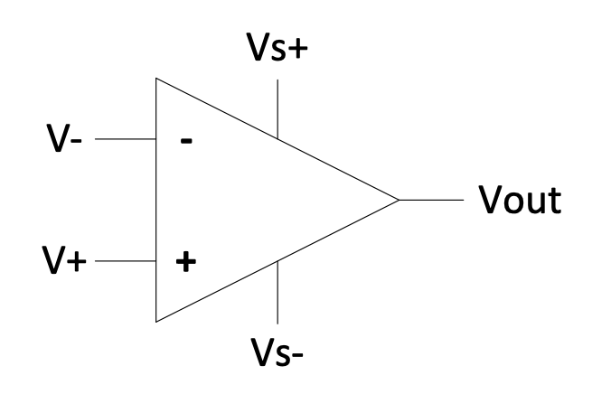 Figure 2.4: Powered op-amp comparator circuit
- If $V_+ > V_-$: $V_{out}$ is high
- If $V_- > V_+$: $V_{out}$ is low
‘High’ means “a voltage close to $V_{s+}$” and ‘low’ means “a voltage close to $V_{s-}$”.
Consider the following circuit:
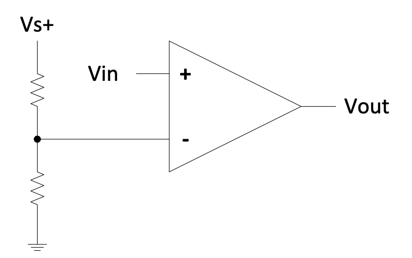 Figure 2.5: Comparator circuit with voltage divider
If the voltage at $V_+$ is larger then the voltage at $V_-$ , which is generated by the resistor divider, then the output will go high. Else the output will go low.
The Window Comparator
The function of the Window Comparator is to indicate when a signal ($V_{in}$ in this circuit) is between two limits.
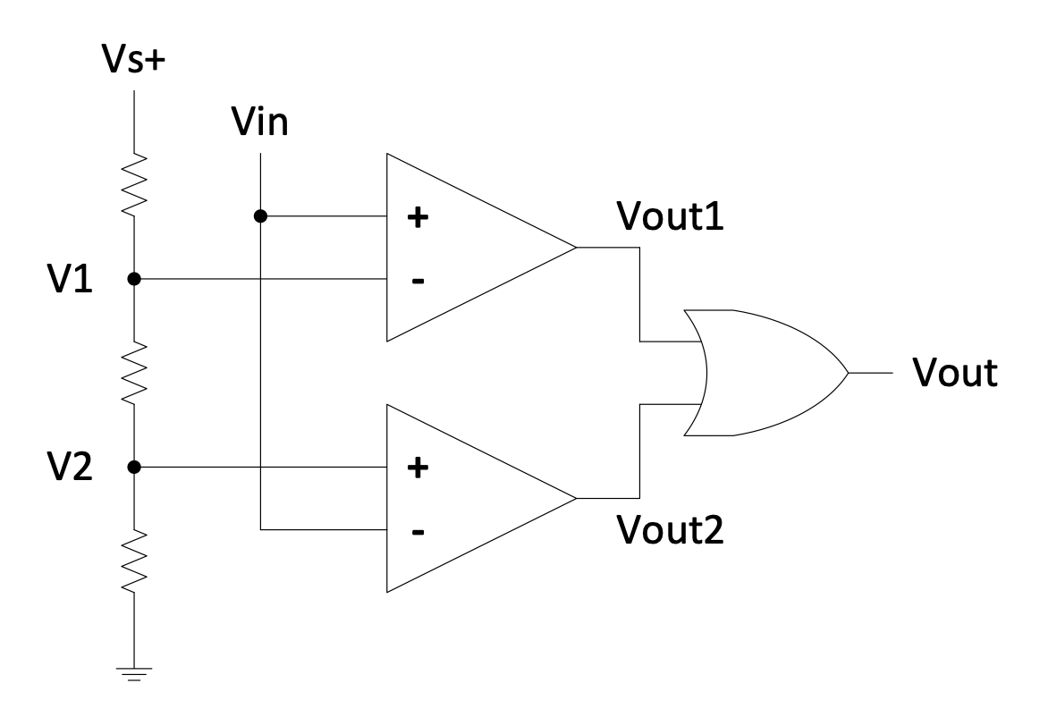 Figure 2.6: Window comparator circuit
- If $V_{in} > V_1$: $V_{out1}$ is high
- If $V_{in} < V_2$: $V_{out2}$ is high
Thus if $V_{in}$ is within the limits of $V_1$ and $V_2$, the output of the OR gate is low.
It can be used to drive a light (like a red LED) indicating when a signal is out of limits.
Question 2.1
Design an equivalent Window Comparator, by swopping the inputs to the op-amps and by using a NAND gate.
The Inverting Amplifier
In this circuit, if the output pin of the op-amp were to change then the inverting input of the op-amp would change in the same direction. You can see this by considering R1 and R2 as a voltage divider. Because of this we have negative feedback.
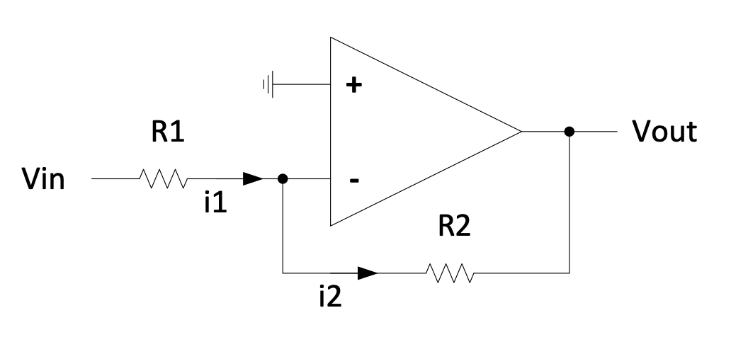 Figure 2.7: Inverting amplifier circuit
Because we have negative feedback we can say that the inverting input will be forced to the same voltage as the non-inverting input (the output can clearly have no influence on the non-inverting input). Thus the inverting input will be forced to 0 V.
$i_1=\frac{V_{in}-0}{R_1}=i_2$ (if we assume that the inputs of the op-amp draw no current) $$V_{across\ R2}=R_2i_2=\frac{V_{in}R_2}{R_1}$$ One end of $R_2$ is at 0 V, current flows from a more positive to a more negative potential: $$\therefore V_{out}=0-\frac{V_{in}R_2}{R_1}$$ Gain is the ratio of the output voltage to the input voltage:
$$Gain=\frac{V_{out}}{V_{in}}=-\frac{R_2}{R_1}$$
We can set the gain of the circuit independently of $A_{v}$ simply with the ratio of resistors (because $A_{v}$ is very large and the current flowing into $V_-$ is very small).
Since the gain is negative we call this circuit an inverting amplifier.
The Non-Inverting Amplifier
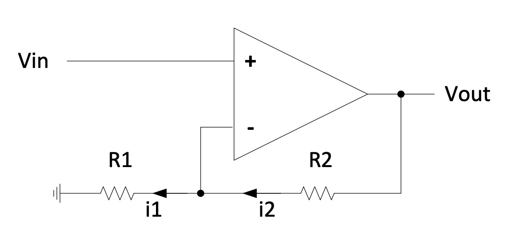 Figure 2.8: Non-inverting amplifier circuit
Negative feedback is present, so the negative input of the op-amp will be driven to $V_{in}$.
By Ohm’s Law: $i_1=\frac{V_{in}}{R_1}$
By KCL: $i_{2} = i_{1}$ $$\therefore V_{acrossR2}=i_2R_2=\frac{V_{in}R_2}{R_1}$$ By KVL: $$V_{out}=V_{acrossR1}+V_{acrossR2}$$ $$=V_{in}+\frac{V_{in}R_2}{R_1}$$ $$=V_{in}(1+\frac{R_2}{R_1})$$
$$Gain=\frac{V_{out}}{V_{in}}=1+\frac{R_2}{R_1}$$
No inversion occurs and the minimum gain is 1.
Once again you should note that the op-amp parameters have no effect on the circuit’s gain (because $A_{v}$ is very large and the current flowing into $V_{-}$ is very small).
The Differential Amplifier
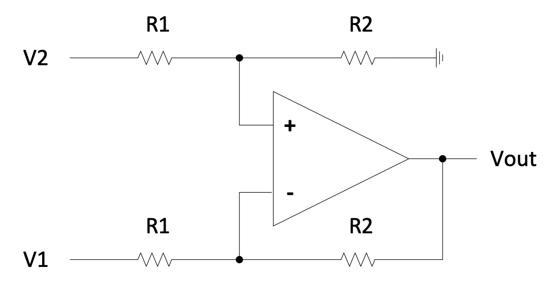 Figure 2.9: Differential amplifier circuit
$$V_{out}=\frac{R_2}{R_1}(V_2-V_1)$$
This circuit is useful for signal conditioning (for example with common noise present on $V_{1}$ and $V_{2}$) as well as for subtracting offsets from signals.
Question 2.2
Derive the equation given above.
A general differential amplifier is discussed in the next sub-section “A short-cut method”.
You do not normally get very high precision from the circuit above because of the difficulty of matching resistors.
If very high precision is needed you can use an “instrumentation amplifier” such as the AD620 or INA110. It has very accurate internal resistors such as $R_{1}$, $R_{2}$ and $R_{3}$ in the following schematic of a typical instrumentation amplifier. $R_{gain}$ is external and adjusts the common gain.
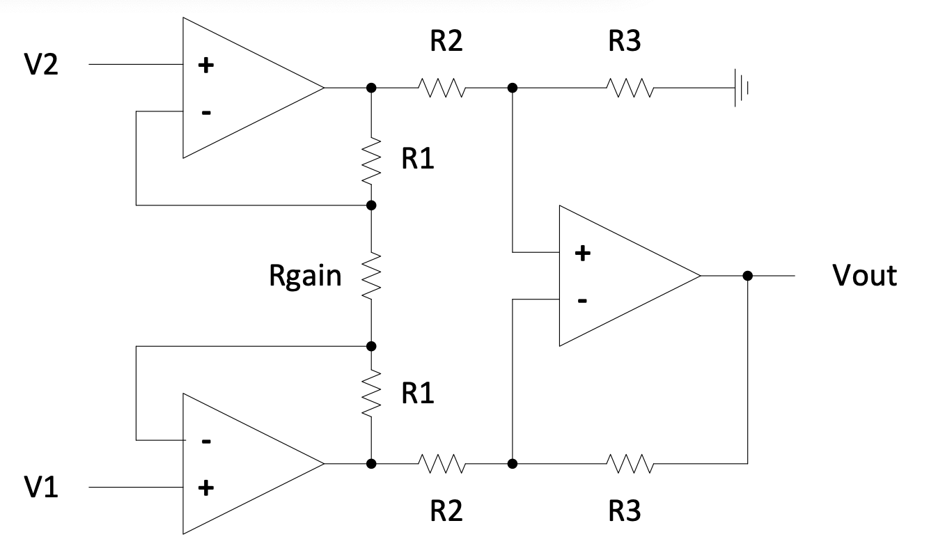 Figure 2.10: Instrumentation amplifier circuit
You don’t have to memorize this equation, but here it is: $$\frac{V_{out}}{V_2-V_1}=(1+\frac{2R_1}{R_{gain}})\frac{R_3}{R_2}$$ Check that if $R_{gain}$ is left out, the gain is $\frac{R_3}{R_2}$ .
Question 2.2b
Why can the last statement be made, from the equation and from the circuit?
A short-cut method
Consider the following network:
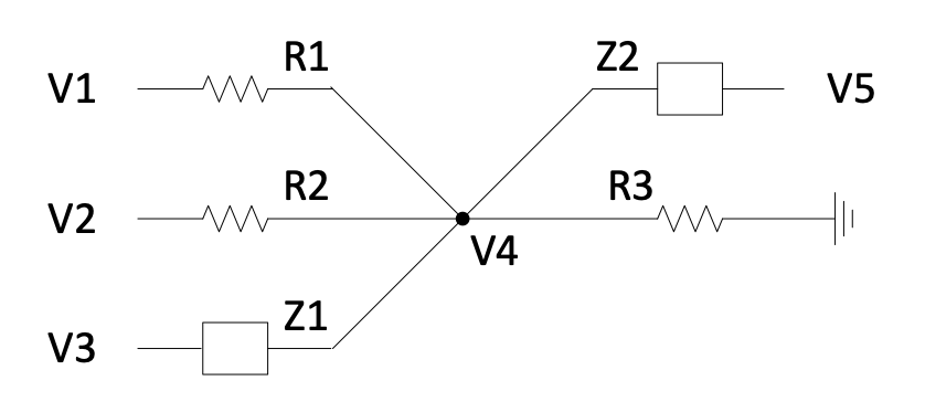 Figure 2.11: Example network for short-cut method
The sum of all the currents flowing into any one point should be zero (KCL).
$$\frac{V_1-V_4}{R_1} + \frac{V_2-V_4}{R_2} + \frac{V_3-V_4}{Z_1} + \frac{V_5-V_4}{Z_2} + \frac{-V_4}{R_3} = 0$$
Re-arranged:
$$V_4\left(\frac{1}{R_1} + \frac{1}{R_2} + \frac{1}{Z_1} + \frac{1}{Z_2} + \frac{1}{R_3}\right) = \frac{V_1}{R_1} + \frac{V_2}{R_2} + \frac{V_3}{Z_1} + \frac{V_5}{Z_2}$$
$$= \frac{V_1}{R_1} + \frac{V_2}{R_2} + \frac{V_3}{Z_1} + \frac{V_5}{Z_2}$$
$$= \frac{V_1}{R_1} + \frac{V_2}{R_2} + \frac{V_3}{Z_1} \text{ (if } Z_2 \to \infty \text{)}$$
$$\therefore V_4\left(\frac{1}{R_1} + \frac{1}{R_2} + \frac{1}{Z_1} + \frac{1}{R_3} + \cdots\right) = \frac{V_1}{R_1} + \frac{V_2}{R_2} + \frac{V_3}{Z_1} + \cdots,$$
And so, in general, assuming $V_n$ is the node voltage in question (e.g. $V_4$ in the above example), and it is connected to $N$ other nodes with voltages $V_i$ through impedances $Z_i$:
$$ V_n \sum_{i=1}^{N} \frac{1}{Z_i} = \sum_{i=1}^{N} \frac{V_i}{Z_i} $$
This is the rule of the short-cut method.
The left-hand side of the equation can be applied to any high impedance point in a circuit.
Note that Z represents a complex impedance used in frequency domain (phasor) analysis. It can be equal to $R, sL, 1/(sC), R+sL, R+1/(sC)$ — in fact, any impedance.
”s” in these terms is the Laplace operator. It is connected to frequency by the equation $s=j\omega$, with $j$ the imaginary number $\sqrt{-1}$ and $\omega = 2\pi f$, with $\omega$ in rad/s and f in Hz.
Note: In electrical engineering, $j$ is used instead of $i$ for the imaginary unit to avoid confusion with current.
If you have a gain or a transfer as a function of Laplace s:
- Replacing $s = 0$ will give you the gain at DC or very low frequencies.
- Replacing $s \to \infty$ will give you the gain at very high frequencies.
For this course you must memorize that:
- The impedance of an inductor $=sL$, with $L$ the inductance in H (henry) [you should be familiar with $i\omega$L as the impedance]
- The impedance of a capacitor $={1}/{(sC)}$ , with $C$ the capacitance in F (farad) [you should be familiar with 1/(i$\omega$C) as the impedance]
- The impedance of two components connected in series is the sum of the two impedances
- $1/s$ is representing an integral
As a first example, apply the short-cut method to an inverting gain op-amp network:
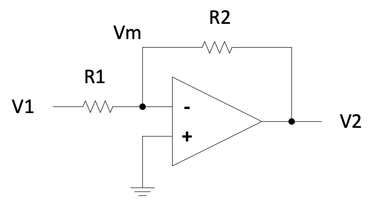 Figure 2.12: Inverting gain op-amp network
$$V_m\left(\frac{1}{R_1} + \frac{1}{R_2} + \frac{1}{Z_{opamp}}\right) = \frac{V_1}{R_1} + \frac{V_2}{R_2} + \frac{V?}{Z_{opamp}}$$
$$\therefore V_m\left(\frac{1}{R_1} + \frac{1}{R_2}\right) = \frac{V_1}{R_1} + \frac{V_2}{R_2} \text{ because } Z_{opamp} \to \infty$$
But $V_{m} = 0$ because the +input of the op-amp is connected to ground and the –input will equal the +input. The –input will equal the +input because of the very high gain of the op-amp and the feedback to the –input of the op-amp.
$$\text{Therefore } 0 = \frac{V_1}{R_1} + \frac{V_2}{R_2}$$
$$\therefore V_2 = V_1\left(-\frac{R_2}{R_1}\right) \quad \therefore \frac{V_2}{V_1} = -\frac{R_2}{R_1}$$
Non-inverting gain:
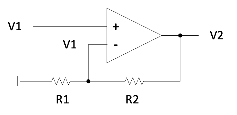 Figure 2.14: Non-inverting gain circuit
$$V_1\left(\frac{1}{R_1} + \frac{1}{R_2}\right) = V_2\left(\frac{1}{R_2}\right) \quad \therefore \frac{V_2}{V_1} = \frac{\frac{1}{R_1}+\frac{1}{R_2}}{\frac{1}{R_2}} = 1 + \frac{R_2}{R_1}$$
Adder or Summer:
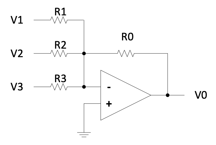 Figure 2.15: Adder or summer circuit
$$0 \times \left(\frac{1}{R_1} + \frac{1}{R_2} + \frac{1}{R_3} + \frac{1}{R_0}\right) = 0 = V_1\left(\frac{1}{R_1}\right) + V_2\left(\frac{1}{R_2}\right) + V_3\left(\frac{1}{R_3}\right) + V_0\left(\frac{1}{R_0}\right)$$
$$\therefore V_0 = -\left(\frac{R_0}{R_1}V_1 + \frac{R_0}{R_2}V_2 + \frac{R_0}{R_3}V_3\right)$$
General differential gain:
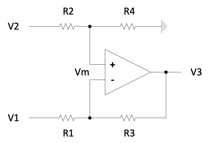 Figure 2.16: General differential gain circuit
$$V_m\left(\frac{1}{R_2} + \frac{1}{R_4}\right) = V_2\left(\frac{1}{R_2}\right) \text{ and }$$
$$V_m\left(\frac{1}{R_1} + \frac{1}{R_3}\right) = V_1\left(\frac{1}{R_1}\right) + V_3\left(\frac{1}{R_3}\right)$$
$$\therefore V_2\frac{\frac{1}{R_2}}{\frac{1}{R_2}+\frac{1}{R_4}} = V_1\frac{\frac{1}{R_1}}{\frac{1}{R_1}+\frac{1}{R_3}} + V_3\frac{\frac{1}{R_3}}{\frac{1}{R_1}+\frac{1}{R_3}}$$
$$\therefore V_3\frac{R_1}{R_1+R_3} = V_2\frac{R_4}{R_2+R_4} - V_1\frac{R_3}{R_1+R_3}$$
$$\therefore V_3 = V_2\frac{R_4}{R_1}\left(\frac{R_1+R_3}{R_2+R_4}\right) - V_1\frac{R_3}{R_1} = V_2\frac{R_4}{R_2}\left(\frac{1+\frac{R_3}{R_1}}{1+\frac{R_4}{R_2}}\right) - V_1\frac{R_3}{R_1} = V_2\frac{1+\frac{R_3}{R_1}}{1+\frac{R_2}{R_4}} - V_1\frac{R_3}{R_1}$$
Check if it complies with your existing knowledge of a differential gain where $R_4=R_3$ and $R_2=R_1$:
$$\frac{V_3}{V_2-V_1} = \frac{R_3}{R_1} \quad \checkmark$$
Trying to derive the equation for the general differential gain without the short-cut method, will demonstrate how many lesser steps are required with the short-cut method.
Integrator:
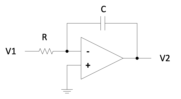 Figure 2.17: Integrator circuit
$$0 = V_1\left(\frac{1}{R}\right) + V_2(sC)$$
$$\therefore \frac{V_2}{V_1} = -\frac{1}{sRC}$$
This is an integrator with a gain of $-\frac{1}{RC}$.
Check: $\left.\frac{V_2}{V_1}\right|_{s=0} \to -\infty \quad \checkmark$
| $\left.\frac{V_2}{V_1}\right | _{s \to \infty} \to 0 \quad \checkmark$ |
1st order low-pass filter:
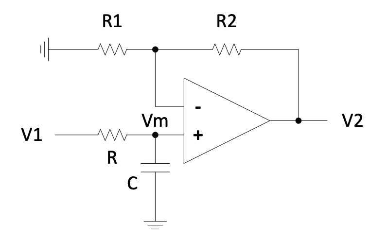 Figure 2.18: 1st order low-pass filter circuit
$$V_m\left(\frac{1}{R_1} + \frac{1}{R_2}\right) = V_2\left(\frac{1}{R_2}\right) \text{ and }$$
$$V_m\left(\frac{1}{R} + sC\right) = V_1\left(\frac{1}{R}\right)$$
$$\therefore V_2\frac{\frac{1}{R_2}}{\frac{1}{R_1}+\frac{1}{R_2}} = V_1\frac{\frac{1}{R}}{\frac{1}{R}+sC}$$
$$\therefore \frac{V_2}{V_1} = \left(1+\frac{R_2}{R_1}\right)\frac{1}{sRC+1} = \frac{K}{\tau s+1} = \frac{K\omega}{s+\omega}$$
This is a 1st order low-pass filter with time constant $\tau$ of $RC$ and low frequency gain $K$ of $1+\frac{R_2}{R_1}$.
Remember bandwidth or cut-off frequency $\omega = 2\pi f = \frac{1}{\tau}$, with $\omega$ in rad/s, $f$ in Hz and $\tau$ in s (seconds).
$\frac{K\omega}{s+\omega}$ is the form of a 1st order low-pass filter with a DC gain of K.
Check: $$\left.\frac{V_2}{V_1}\right|_{s=0} = 1+\frac{R_2}{R_1} \quad \checkmark$$
| $$\left.\frac{V_2}{V_1}\right | _{s \to \infty} \to 0 \quad \checkmark$$ |
Therefore, at low frequency there will be a gain greater than 1.0, but at higher frequency, the gain will become smaller and smaller. So it is indeed a low-pass filter.
Combining Op-amp circuitry with Transistors
It is often required that a signal must be amplified and then it must drive a load that requires more current than what an op-amp can supply. Therefore a transistor must be combined with the op-amp. Both the following circuits may work, but the second one will be more accurate.
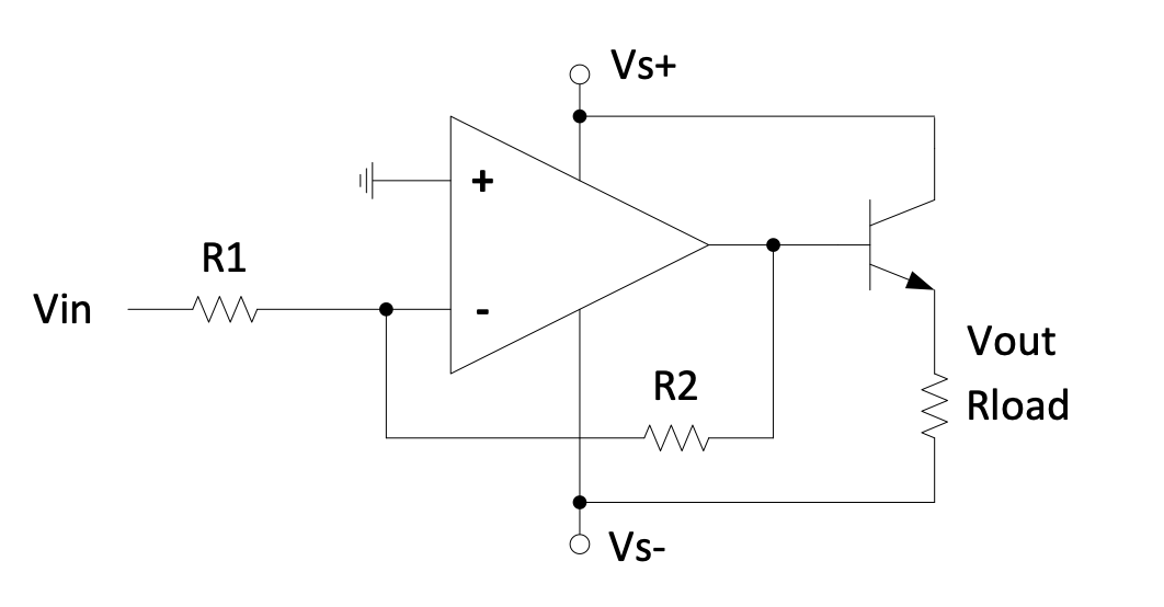 Figure 2.19: Inverting amplifier circuit with transistor
Question 2.3
Do you agree with the equation: $$V_{out} = -\frac{R_2}{R_1}V_{in} - 0.7$$
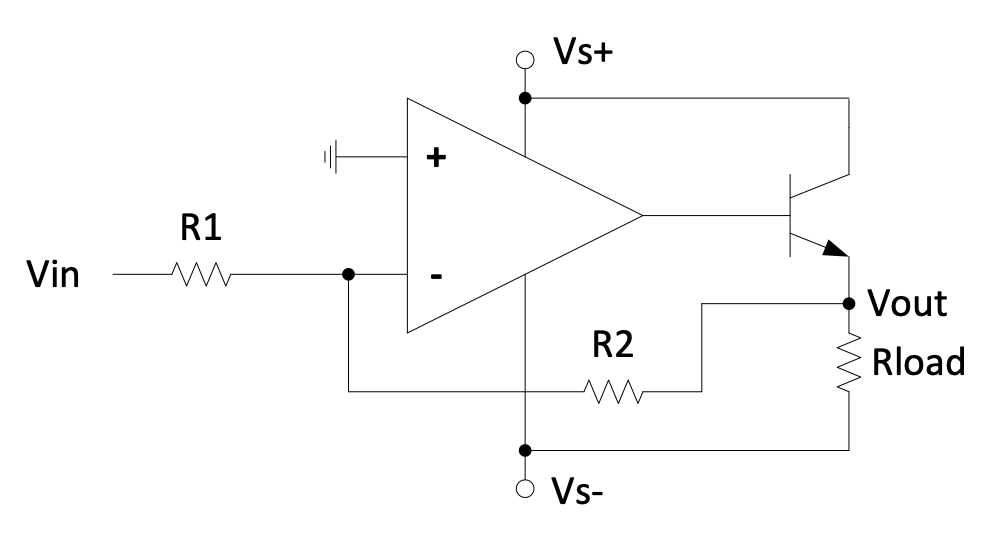 Figure 2.20: More accurate inverting amplifier circuit with transistor
Question 2.4
Do you agree with the equation: $$V_{out} = -\frac{R_2}{R_1}V_{in}$$ What happened to the 0.7 V in the last case?
Question 2.5
How would you combine NPN and PNP transistors with an Op-amp to allow positive and negative current through the load?
Designing and selecting components
Resistors, capacitors, inductors and zener diodes come only in certain values, also depending on the accuracy of the components. These are given in the Appendix “Number series…”
It is obvious from the transfer functions derived above, that different orders of for example resistors can give the same transfer function on the first look. For example, $\frac{33\,\Omega}{10\,\Omega} = \frac{33\,k\Omega}{10\,k\Omega}$. But there are obvious reasons why the $k\Omega$ resistors is a far better choice when working with op-amps than the $\Omega$ only resistors:
-
For given voltages, larger resistors dissipate less power than smaller resistors – wasting energy is not sensible.
-
Op-amps can only supply or sink current in the order of 10 mA, so with resistors in the $\Omega$ only range only very small signals can be handled.
Single Supply and Dual Supply Op-amps
For an op-amp to work correctly $\textit{all}$ inputs and the output of the op-amp must be within its allowable range. This range is constrained by the power supply rails.
For a common dual rail op-amp (e.g. LM741) neither the input nor output voltages will exactly go from rail to rail.
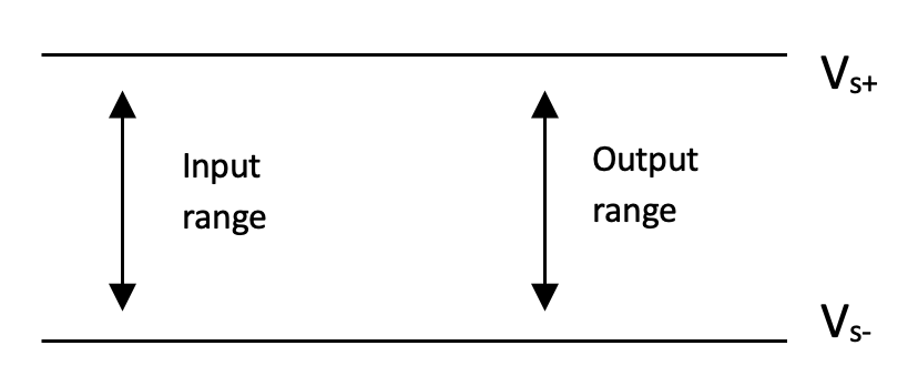 Figure 2.21: Input/output voltage range for dual supply op-amp
The difference between the dual supply device and the single supply device is in the allowable input voltage range relative to the supply voltages.
For a single supply op-amp (e.g. LM358, $V_{s-}$ is usually ground):
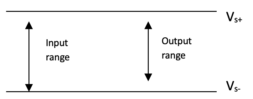 Figure 2.22: Input/output voltage range for single supply op-amp
Note: Although the input is shown here to be as low as on $V_{s-}$, it must still be slightly bigger than $V_{s-}$.
Why are single supply op-amps useful?
Simply because dual supplies are more expensive and require more space.
Can you use dual supplies on a single supply op-amp? Yes, provided you don’t exceed the maximum total supply voltage ($V_{s+} - V_{s-}$) allowed for the op-amp.
Single supply op-amps, such as the LM358, will give some distortions when crossing over from positive to negative or negative to positive current on its output. A dual supply op-amp, such as the LF353 won’t display this distortion.
Consider the circuit below, with $V_+ = 10\,\text{V}$, assuming the specification: $0.5\,\text{V} \leq V_{out} \leq 9.5\,\text{V}$:
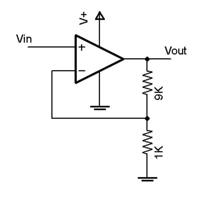 Figure 2.23: Dual supply op-amp example circuit
- The allowable range for $V_{in}$ is from 0.05 V to 0.95 V (restricted by the limited range of $V_{out}$).
But the input to an op-amp circuit usually has different restrictions than the inputs to the op-amp themselves.
Consider this circuit with a single supply op-amp:
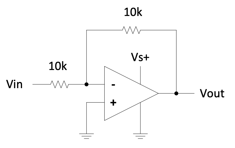 Figure 2.24: Single supply op-amp example circuit
$V_{in}$ can be negative because that will cause $V_{out}$ to be positive. $V_{-}$ will be forced to ground and thus, from the op-amp’s point of view, all signals are in the allowable range.
But in this latter case $V_{in}$ can’t be positive because $V_{out}$ can’t be negative.
Special rail to rail op-amps are available that will allow both input and output voltages to swing almost to both supply rails. These op-amps use MOSFETs internally instead of transistors. They have smaller saturation voltages than transistors.
The Non-Ideal Op-amp
Input Offset Voltage
One of the properties of a real-life op-amp that will cause deviation from the model is that an op-amp used in negative feedback will not be able to drive both its inputs to the exact same voltage. Input Offset voltage specifies the maximum voltage difference between the inputs when the op-amp is in negative feedback mode.
Input Bias Current
We also assumed that no current flowed into the inputs. In reality some current will. This current is called the input bias current and because the two inputs might not draw identical currents, this value is the average of the two inputs.
Gain Bandwidth Limits
All op-amps have a specification called Gain Bandwidth Product (GBWP). This is a constant for that device and it is measured in MHz. The product of the open loop gain of the op-amp and the frequency of operation is roughly constant.
Thus, as the operating frequency goes up, the open loop gain goes down.
E.g. the LM358: GBWP = 1 MHz
Up to 10 Hz: $A_v = 100\,000$
At 1 kHz: $A_v = 1000$
At 10 kHz: $A_v = 100$ etc.
We originally assumed that $A_v$ was infinite for our analysis of op-amp behaviour. If $A_v$ is less, then overall performance will deteriorate.
As a rule of thumb keep the closed loop gain of the op-amp circuit $< A_v/10$.
Slew Rate Limitation
The “slew rate” of an op-amp is the maximum rate of change of its output. It is typically specified in V/µs. The LM358 has a slew rate of 0.5 V/µs.
Thus, if the LM358’s output had to swing sharply from 0 V to 5 V the output waveform would look like this:
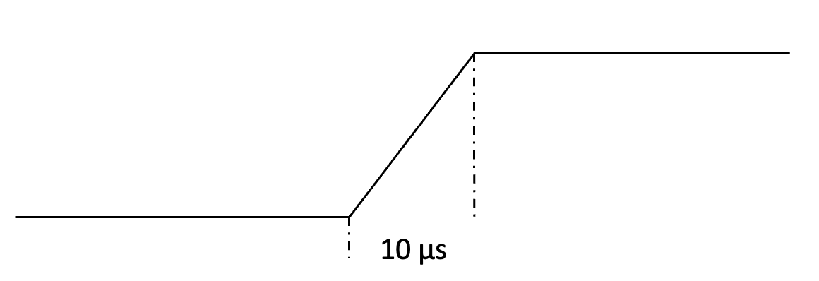 Figure 2.25: Slew rate limitation
This will distort square edges and limits the frequency of operation in comparator applications.
Dedicated Comparator Circuits
There are devices called comparators which are similar to op-amps but are used in applications where the output is only high or low. Examples include the LM311 and LM393. They often have “open collector” and “open emitter” outputs.
To use them you have to connect the collector to the supply and a pull-down resistor from the emitter to ground (the second diagram below). So this is a comparator followed by an emitter follower. It can also be connected as in the first diagram, with then the output the inverse of the circuit of the second diagram.
Their slew rate can be as high as 30 V/µs.
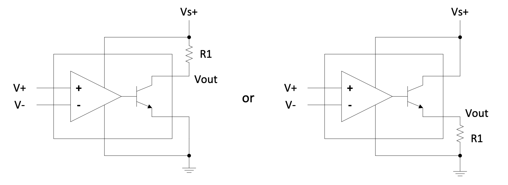 Figure 2.26: Dedicated comparator circuits
Remember that the output pin will have some parasitic capacitance. This will slow down the maximum possible rate of change of the output. The rise time can be reduced by reducing $R_1$ at the cost of larger current wastage through the comparator’s output. Typically $R_1$ will be about 1k.
The first diagram looks suspicious in terms of the comparator component output driving the transistor without any resistor. Presumably the comparator output has sufficient internal resistance.
Hysteresis
Hysteresis is an important aspect in controlling devices.
Suppose that we are using an op-amp as a comparator to control a cooling fan. If temperature $> 50^\circ\text{C}$ the fan must be on. Suppose the temperature sensor outputs 2.5 V at $50^\circ\text{C}$. We can put together the following circuit (the reason for the 2 transistors is to eventually be able to supply sufficient current to the fan):
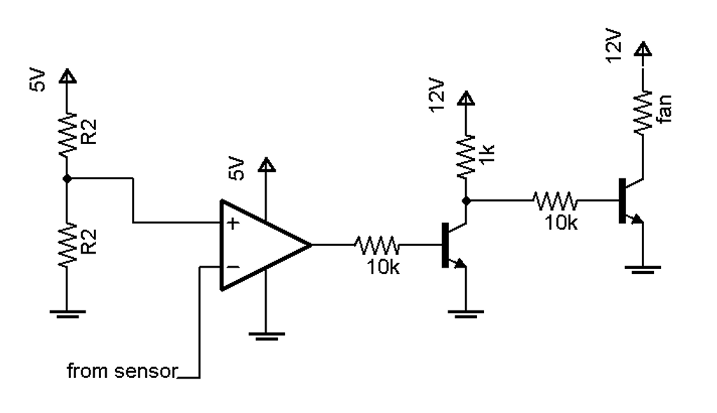 Figure 2.27: Hysteresis example circuit
When the fan turns on it causes the temperature to drop, which will then turn the fan off, which causes the temperature to rise etc... The problem is that the fan will turn on and off very rapidly which is not good for it. We can fix this problem by using positive feedback or hysteresis.
Therefore, take note that positive feedback may sometimes be useful. The amplifier (comparator in this case) is then not running in the linear mode, since its output will either be maximum or minimum, never in between except when switching from one extreme to the other as fast as it can.
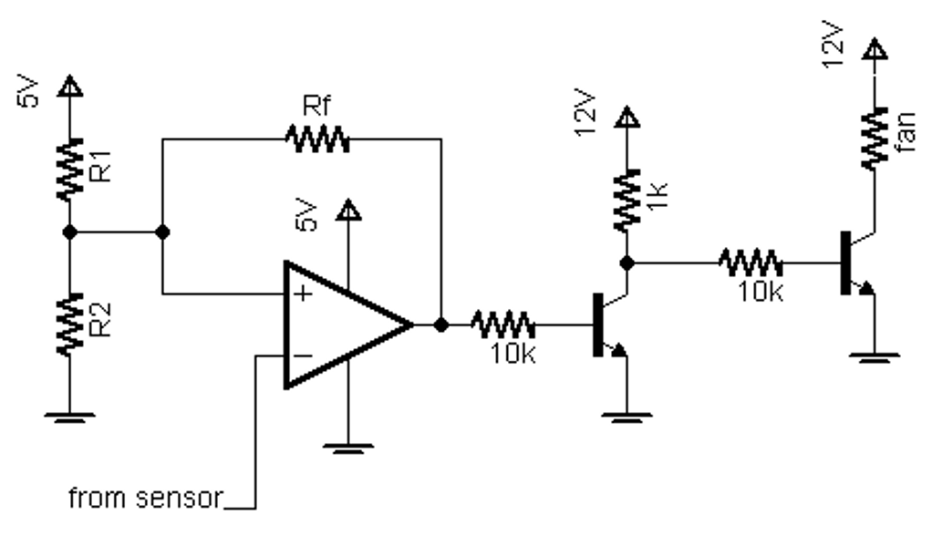 Figure 2.28: Hysteresis example circuit with positive feedback
The output of the op-amp now affects the reference level (the $V_+$ input of the comparator). When the fan is on there is a threshold below $50^\circ\text{C}$ and when the fan is off the threshold is above $50^\circ\text{C}$.
If you want to calculate the thresholds remember that if the op-amp’s output is high, $R_f$ is effectively in parallel with $R_1$ and when it is low $R_f$ is effectively in parallel with $R_2$. This can be used to calculate the reference voltages, unless you must work more accurately by taking into account that the output of the comparator won’t be exactly 0 V or 5V. The short-cut method can also be used, which I would recommend, since it can also handle this more accurate analysis. It can even handle the case where $R_1$ and $R_2$ are not given, but must be calculated – see the tips below.
Question 2.6
Suppose a temperature sensor of 0.1 V/$^\circ\text{C}$ with output 2.5 V at $50^\circ\text{C}$. Let $R_1=R_2=10\,\text{k}\Omega$. Design $R_f$ so that the thresholds for controlling the fan will be at $47^\circ\text{C}$ and $53^\circ\text{C}$. Do the design for two cases:
- Output of comparator is either 0 V or 5 V
- Output of comparator is either 0.2 V or 4.8 V
Tips: $$V_{sensor}\left(\frac{1}{R_1}+\frac{1}{R_2}+\frac{1}{R_f}\right)=5\left(\frac{1}{R_1}\right)+V_0\left(\frac{1}{R_f}\right)$$ and apply this at the two given conditions:
- $V_{sensor}$ corresponding with the low temperature, while $V_0$ the low voltage
- $V_{sensor}$ corresponding with the high temperature, while $V_0$ the high voltage
In the most general case, this will give you 2 equations and 3 unknowns: $R_1$, $R_2$ and $R_f$.
Example solutions
Solutions to the examples in this section can be found here.