Chapter 4: Filter Circuits
Table of Contents
-
Chapter 4: Filter Circuits
- Noise
- Decoupling Capacitors, Capacitive Coupling
- Filter Revision
- Example solutions
Often, we have small signals which we need to measure. We need to apply some special techniques in order to preserve these.
Noise
Noise is one of the biggest problems we have in dealing with small signals. We have 2 basic types of noise:
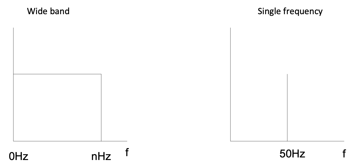 Figure 4.1: Noise types
Of course, ideal properties are shown on the graphs – in practice the noise will taper off against frequency, and single frequencies will have harmonics (multiples of the base frequency) as well. The best approach is to try and stop the noise from getting into the system and thus eliminate it completely. Noise comes from several sources. It can be radiated into a system or it can be generated by components.
Internal noise or component noise consists of:
-
Thermal noise: Any temperature above absolute zero causes electrons to move resulting in thermal noise. This can be reduced by cooling down the system.
-
Shot Noise: This noise is caused by the nature of current being the movement of discrete charged particles (electrons).
The bigger the resistance of the component the greater the generated noise.
If we choose our components carefully then we can often reduce noise. If high amplification is needed then good quality, low noise components should be used. For example the LM358 op-amp has high noise, but the Ne5532 has low noise. The same can be found with transistors.
External or radiated noise is most common around 50 Hz which is radiated by power conductors. The best way of minimizing this noise is to properly shield your system, including cables, connectors and circuitry.
The simplest method is to place a shield around cables as shown below or use metal casings. There are different quality shields available and some will perform better against noise than others.
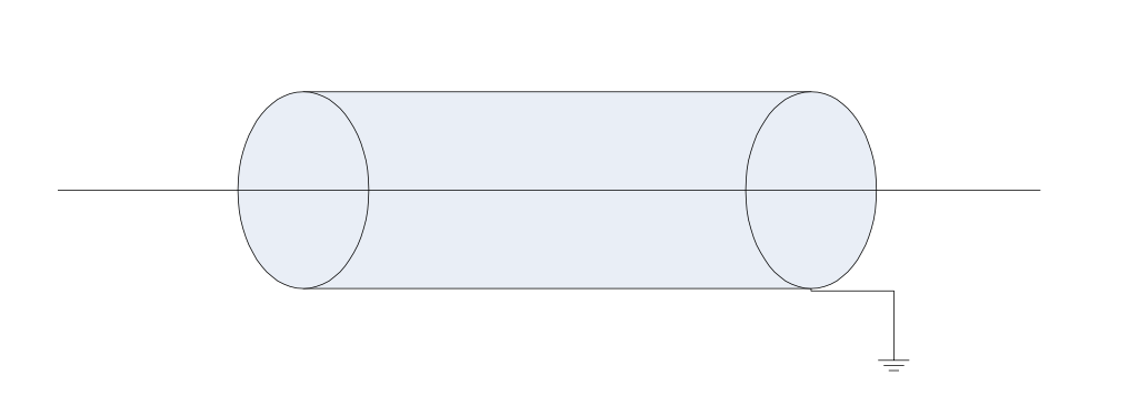 Figure 4.2: Shielded cable
Notice that the shield is connected to ground. Some systems use the shield to carry signals; then it won’t be connected to ground.
We can get even better performance using an impedance balanced differential system. This is done by adding a resistor in the ground line below, with resistance equal to the output resistance of the signal line.
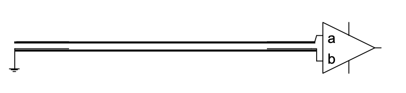 Figure 4.3: Impedance balanced differential system
Any noise that affects line A will also affect line B likewise, not only because they are close together (where twisting them will help even more), but also because they are impedance matched.
The following diagram explains how impedance matching reduces noise.
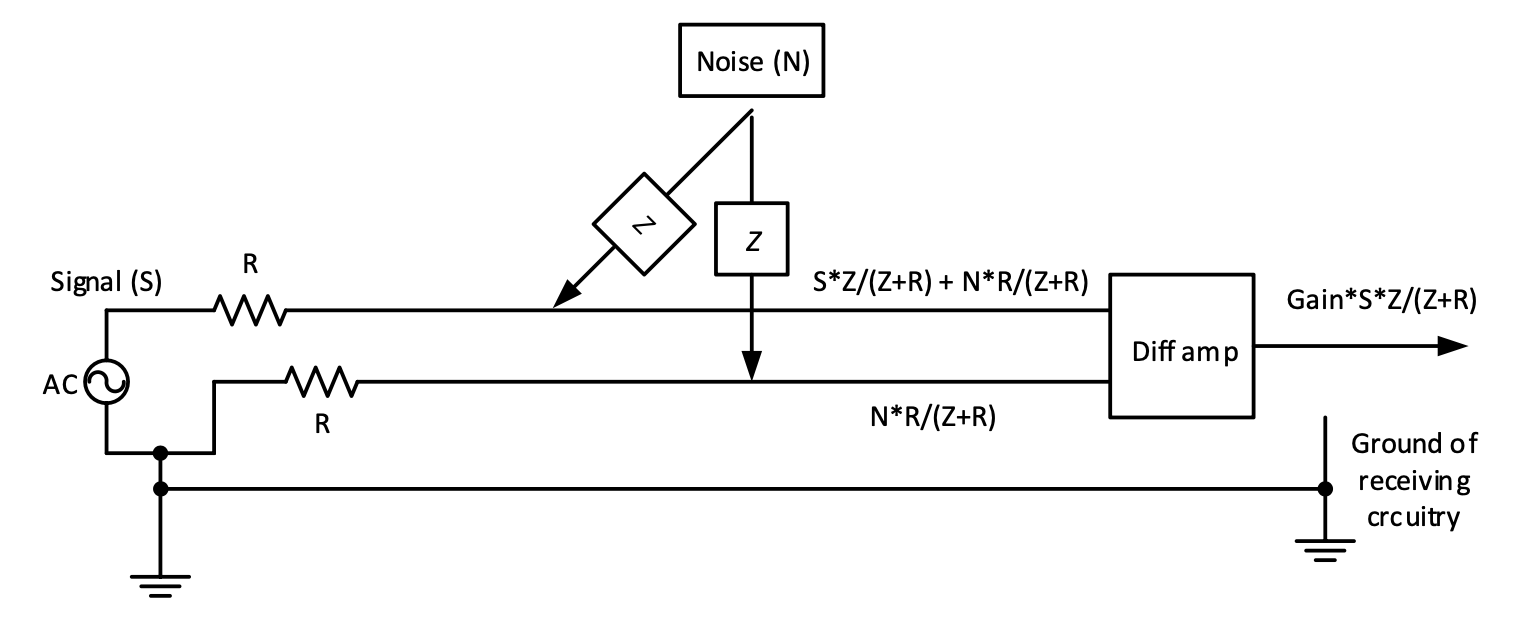 Figure 4.4: Impedance matching
The common noise in line A and line B will be eliminated by the differential amplifier.
Without the added R in the lower line, the output would have been Gain*[S*Z/(Z+R) + N*R/(Z+R)] because there would have been no noise in the lower line.
The best system is to use an impedance matched shielded differential system.
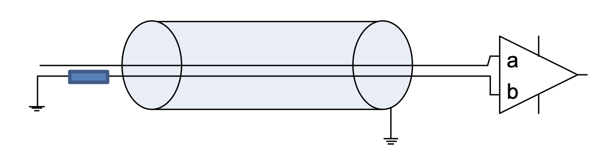 Figure 4.5: Instrumentation amp applied to a differential system in a shielded cable
Instrumentation amps are great for balanced systems. They can provide good quality differential outputs. Ability to reject common signals on a differential amp is called “common mode rejection ratio” CMRR. The better the CMRR specification the better your circuit will reject noise.
Even if we use properly connected and shielded cables, we may still get noise in our system which will have to be removed. One method to do this is by using filters.
Decoupling Capacitors, Capacitive Coupling
You can use decoupling capacitors to smooth off noise from supplies or certain parts of the circuitry. They are connected between the supply and ground. In principle they are like the $1^{st}$ low-pass filter discussed below, with the internal resistance of the power supply acting as the resistor.
Some devices are noisier than others. Anything that switches high current will create noise. Motors are particularly noisy. It is common practise to use more than one capacitor to eliminate noise. Small capacitors are more effective for high frequency, low amplitude noise, while larger ones are better for slow, larger amplitude signal changes. Physical proximity must be considered as well.
You can also enclose each noisy module in a metal box, which will further shield other circuitry from the effects of noise.
Capacitive coupling is when the DC component in a signal is to be taken out while the AC components must pass. This is done by inserting a capacitor in a line in series with the circuitry following. In principle this is like the $1^{st}$ high-pass filter discussed below.
Filter Revision
There are four types of filters we will discuss here. The first two you should have come across before. They are the low-pass filter, and the high-pass filter. The last two will be the band-pass filter and the notch filter. A summary of the basic transfer functions of all 4 these filters are given at the end of this chapter.
The low-pass filter
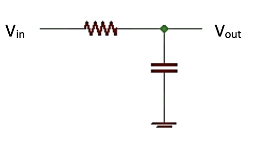 Figure 4.6: Low-pass filter circuit
To analyze a filter we look at its behavior at DC and at an infinite AC frequency.
At DC, there will be a steady voltage at the capacitor (the capacitor charges and holds its voltage). This voltage will be present at the output. Thus at low frequencies $V_{out}$ is almost equal to $V_{in}$.
At very high frequencies the capacitor becomes a short circuit to ground. This means that no voltage will be present at the output.
This filter passes the low frequency signals but reduces the high frequency signals which is why it is called a low-pass filter. It would be used if the frequency of the noise in the system is high. You can set the frequency at which this filter blocks the voltage by choosing different resistor and capacitor combinations.
If we plot the frequency response for a low-pass filter we see that the tail, or end of the graph takes up the most space. However, if we plot the same graph over a logarithmic scale we get a much more convenient result. The Bode plot of a low-pass filter is shown below.
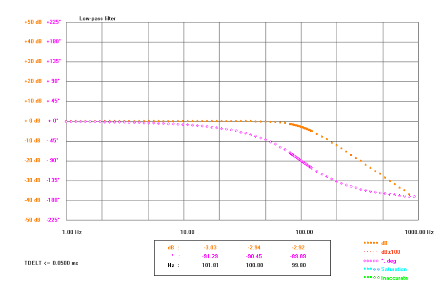 Figure 4.7: Bode plot of a low-pass filter
The transfer function of this low-pass filter is:
$$\frac{V_{out}}{V_{in}} = \frac{\frac{1}{sC}}{R+\frac{1}{sC}} = \frac{1}{1 + sRC} = \frac{1}{\tau s + 1} = \frac{\omega_c}{s + \omega_c}$$
This is a $1^{st}$ order low-pass filter with bandwidth or cut-off frequency $\omega_c = \frac{1}{RC}$ rad/s and low frequency gain of 1.
$\mathbf{\frac{\omega_c}{s + \omega_c}}$ is the form of a $1^{st}$ order low-pass filter with a DC gain of 1.
Note that a load like a resistor to ground will change the transfer of this filter, so a load connected to this must be of high impedance or the transfer must be calculated with the load taken into account.
The high-pass filter
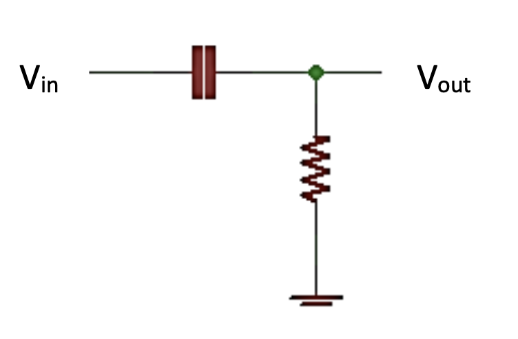 Figure 4.8: High-pass filter circuit
At very high frequencies the capacitor becomes a short circuit from the input to the output. This means that $V_{out}$ will closely match $V_{in}$.
At DC, no current will be allowed through once the capacitor is charged thus no voltage will be present at the output.
This filter passes the high frequencies but stops any low frequencies which is why it is called a high-pass filter. This filter would be used if the frequency of the noise in the system was low and you don’t need to pass on any DC signals. You can set the frequency at which this filter blocks the voltage by choosing different resistor and capacitor combinations.
The Bode plot of a high-pass filter is shown below.
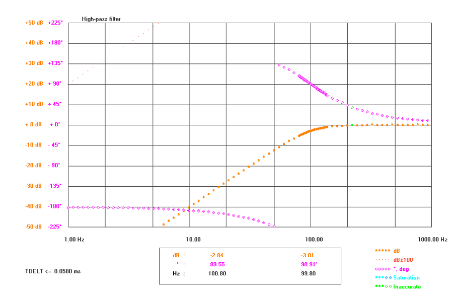 Figure 4.9: Bode plot of a high-pass filter
The transfer function of this high-pass filter is:
$$\frac{V_{out}}{V_{in}} = \frac{R}{R + \frac{1}{(sC)}} = \frac{sRC}{sRC + 1} = \frac{\tau s}{\tau s + 1} = \frac{s}{s + \omega_c}$$
This is a $1^{st}$ order high-pass filter with cut-off frequency $\omega_c = \frac{1}{RC}$ rad/s and high frequency gain of 1.
$\frac{\mathbf{s}}{\mathbf{s + \omega_c}}$ is the form of a $1^{st}$ order high-pass filter with a high frequency gain of 1.
Active $1^{st}$ order low-pass filter
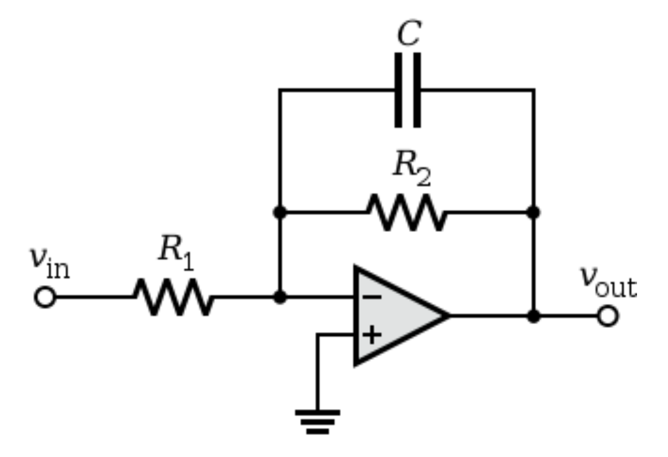 Figure 4.10: Active $1^{st}$ order low-pass filter circuit
Unlike the passive filters above, this one is active because an op-amp is part of it.
Start by looking carefully at the circuit. This is an inverting amplifier with negative feedback with the addition of a capacitor. First analyse this circuit at DC where the capacitor becomes an open circuit. This means we can ignore it when considering DC and the circuit becomes a standard inverting amplifier. If the gain is 1, Vout = Vin. This circuit is very useful to add gain to the output apart from the filtering, and can supply more current than the passive version.
Then analyse this circuit at very high frequencies where the capacitor becomes a short circuit. This means all the current flows through C and none through R2. Since the voltage at the inverting input is zero, the output will be zero.
Clearly there will be a range of frequencies between infinite AC frequency signals and DC signals. For these the capacitor will allow varying amounts of current to flow, reducing the gain of the output.
Apply the short-cut method:
$$0 = V_{in}\left( \frac{1}{R_{1}} \right) + V_{out}\left( \frac{1}{R_{2}} \right) + V_{out}(sC)$$
$$\Rightarrow \frac{V_{out}}{V_{in}} = - \frac{\frac{1}{R_{1}}}{\frac{1}{R_{2}} + sC} = - \frac{\frac{R_{2}}{R_{1}}}{sR_{2}C + 1} = \frac{K}{\tau s + 1} = \frac{K\omega_c}{s + \omega_c}$$
This is a $1^{st}$ order low-pass filter with bandwidth or cut-off frequency $\omega_c = \frac{1}{R_{2}C}$ rad/s and low frequency gain of $- \frac{R_{2}}{R_{1}}$.
$\frac{\mathbf{K\omega_c}}{\mathbf{s + \omega_c}}$ is the form of a $1^{st}$ order low-pass filter with a DC gain of K.
Check the correlation and differences between this filter and the $1^{st}$ order low-pass filter in Chapter 2.
Example 4.1
$$\frac{V_{out}}{V_{in}} = - \frac{\frac{R_{2}}{R_{1}}}{sR_{2}C + 1} = - \frac{\frac{1}{R_{1}C}}{s + \frac{1}{R_{2}C}} = \frac{K\omega_c}{s + \omega_c}$$
Specifications: Cut-off frequency of 80 Hz, $\omega_c = 2\pi80 = 502.7 \ rad/s$
Gain K = -5.0
There are 3 unknowns (components R1, R2 and C), 2 equations, therefore 1 component can be chosen and the remaining 2 components can be calculated and selected from the E12 series – as close as possible or using two instead of one component.
$\frac{1}{R_{1}C} = 5.0 \times 502.7$ and $\frac{1}{R_{2}C} = 502.7$
Choose C = 10 nF, $\Rightarrow R_{1} = 39.79 \ k\Omega$, therefore choose $R_{1} = 39 \ k\Omega$.
$R_{2} = 198.9 \ k\Omega$, therefore choose $R_{2} = 200 \ k\Omega$ (or 100 k$\Omega$ + 100 k$\Omega$).
Therefore the design results are: $R_{1} = 39 \ k\Omega$, $R_{2} = 200 \ k\Omega$, C = 10 nF
Check:
Resulting design parameters:
$\omega_c = \frac{1}{R_{2}C} = 2\pi \times 79.58 = 499.8 \ rad/s$,
$K = - \frac{1}{R_{1}C} \times \frac{1}{2\pi 79.58} = - 5.13$
They are close to the specifications.
$\omega_c\ \%\ error = \frac{79.58 - 80}{80} \times 100\% = - 0.52\%$
$K\ \%\ error = \frac{- 5.13 - ( - 5.0)}{- 5.0} \times 100\% = + 2.6\%$
$|K|\ \%\ error = \frac{5.13 - 5.0}{5.0} \times 100\% = + 2.6\%$
Active $2^{nd}$ order low-pass filter
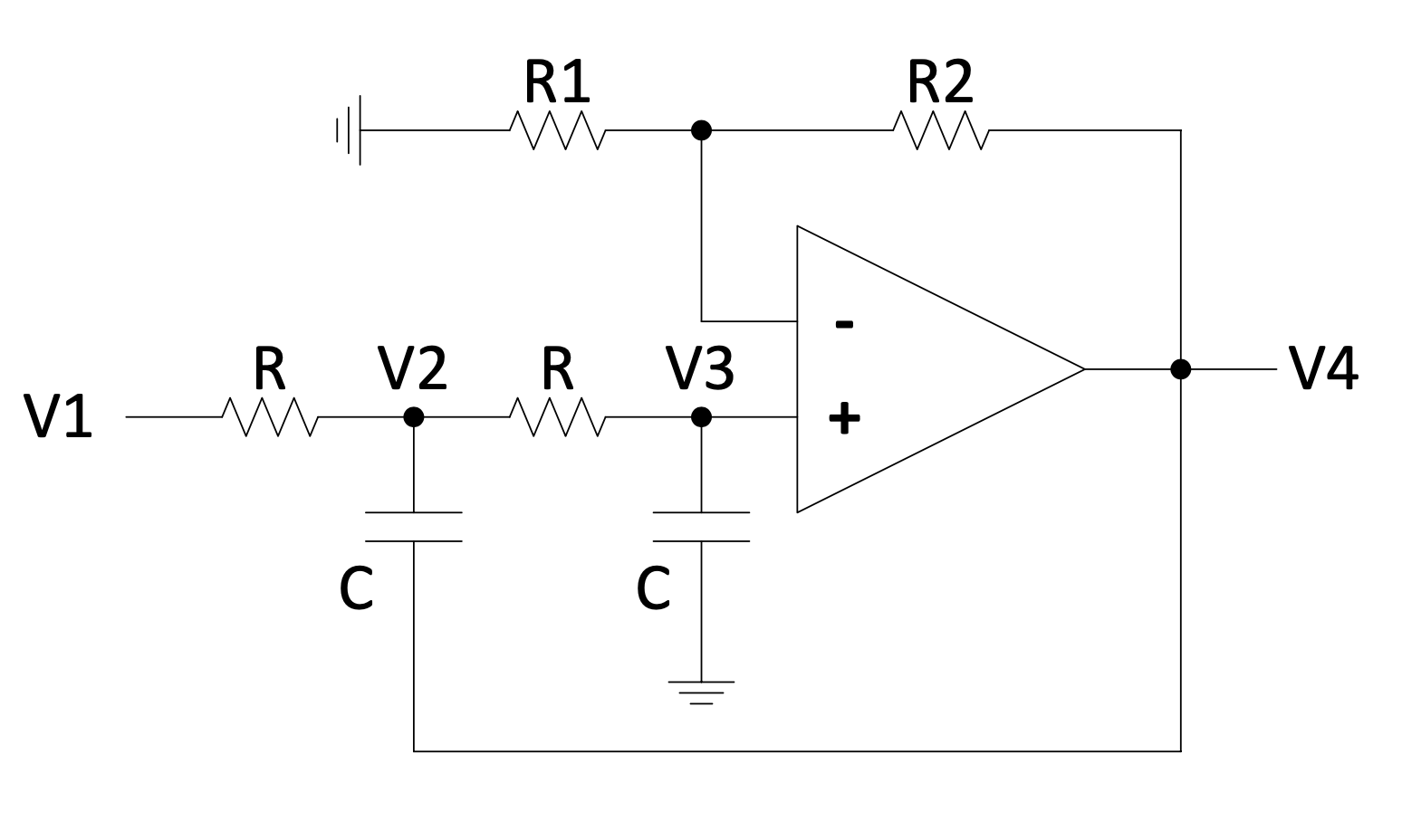 Figure 4.11: Active $2^{nd}$ order low-pass filter circuit
The transfer function for an active $2^{nd}$ order low-pass filter can be calculated with the short-cut method:
$V_{3}(1/R_{1} + 1/R_{2}) = V_{4}(1/R_{2})$; and
$V_{3}(1/R_{1} + sC) = V_{2}(1/R)$
$\Rightarrow V_{3} = V_{4}\frac{R_{1}}{R_{1}+R_{2}}$ and
$V_{4}\frac{R_{1}}{R_{1} + R_{2}} = V_{2}\frac{1}{sRC + 1}$ $V_{2} = V_{4}\frac{R_{1}}{R_{1} + R_{2}}(sRC + 1)$
$V_{2}(1/R_{1} + 1/R_{2} + sC) = V_{1}(1/R_{1}) + V_{3}(1/R_{2}) + V_{4}sC$
$\Rightarrow V_{2}(2+sRC) = V_{1} + V_{3} + V_{4}sRC$
Substitute $V_{2}$ and $V_{3}$ in terms of $V_{4}$:
$V_{4}\frac{R_{1}}{R_{1} + R_{2}}(sRC + 1)(sRC + 2) - V_{4}\frac{R_{1}}{R_{1} + R_{2}} - V_{4}sRC = V_{1}$
Multiply all terms with $1+R_{2}/R_{1}=(R_{1}+R_{2})/R_{1}$:
$V_{4}\left\lbrack s^{2}(RC)^{2} + 3sRC + 1 - sRC\left( 1 + \frac{R_{2}}{R_{1}} \right) \right\rbrack = V_{1}(1 + \frac{R_{2}}{R_{1}})$
$$\Rightarrow \frac{V_{4}}{V_{1}} = \frac{1 + \frac{R_{2}}{R_{1}}}{s^{2}(RC)^{2} + sRC\left( 2 - \frac{R_{2}}{R_{1}} \right) + 1} = \frac{K\omega_{c}^{2}}{s^{2} + 2\zeta\omega_{c} s + \omega_{c}^{2}}$$
This is a $2^{nd}$ order low-pass filter with bandwidth or cut-off frequency $\omega_{c} = \frac{1}{RC}$ rad/s and low frequency gain $K = 1 + \frac{R_{2}}{R_{1}}$.
Check:
$$\left.\frac{V_{4}}{V_{1}}\right|_{s=0} = 1 + \frac{R_2}{R_1} \quad \checkmark$$
$$\left.\frac{V_{4}}{V_{1}}\right|_{s\to \infty} \to 0 \quad \checkmark$$
Although these two checks pass, it is not to say that the transfer function is in all aspects 100%. Before realizing all the components and building it (that would be the ultimate test), it is always good to double check your calculations. But if the simple checks fail, something is obviously wrong.
Comparing the response of the LPF with various damping factors
The figure below shows the response of the LPF with various damping factors compared to a $1^{st}$ order LPF. Here it can be seen that when $\zeta = 0.707$, the response is the flattest. When this is the case the filter is known as a Butterworth filter. When $\zeta > 0.707$, the response is said to be overdamped (a Bessel filter) and there is no resonance. When $\zeta < 0.707$, the response is said to be underdamped (a Chebyshev filter) and there is resonance. Compared to the $1^{st}$ order LPF, the $2^{nd}$ order LPF has a steeper roll-off of -40 dB/decade compared to -20 dB/decade for the $1^{st}$ order LPF.
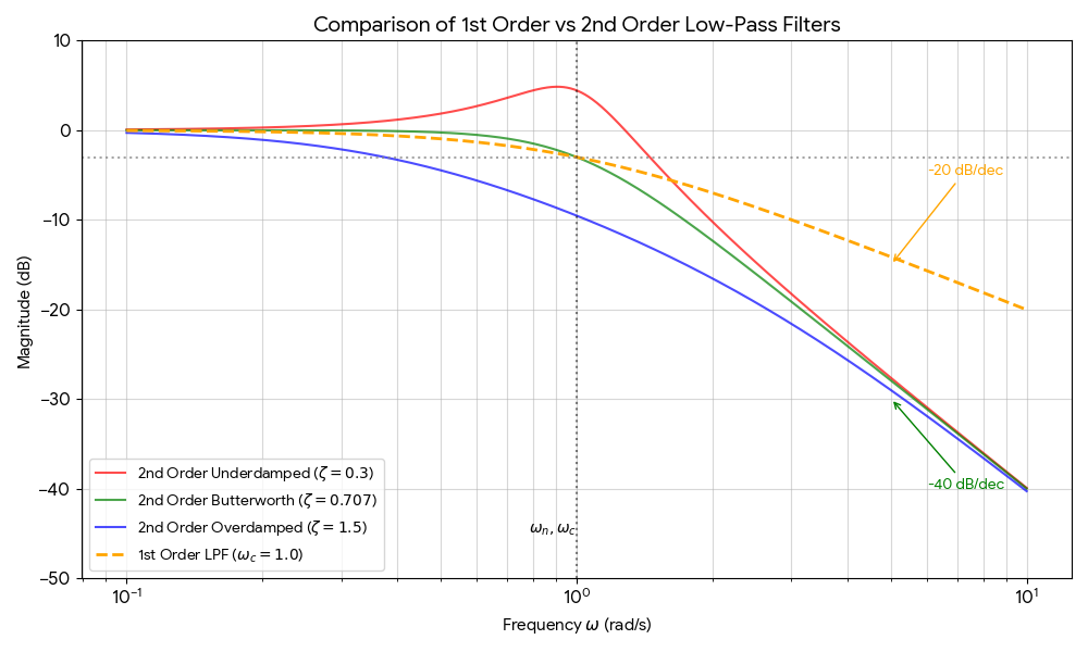
Further, if the cut-off frequency is defined as the frequency where the gain is -3 dB, then it is clear that the damping coefficient $\zeta$ affects the cut-off frequency. And so, the transfer function $\frac{V_{4}}{V_{1}}$ above is only true when $\zeta = 0.707$ (Butterworth filter). Accordingly, we instead, define the general form of a $2^{nd}$ order LPF using the resonance frequency $\omega_n$ rather than the cut-off frequency:
$$\frac{V_{out}}{V_{in}} = \frac{K\omega_n^{2}}{s^{2} + 2\zeta\omega_n s + \omega_n^{2}}$$
(At $\zeta = 0.707$, $\omega_n = \omega_c$).
Active $1^{st}$ order high-pass filter
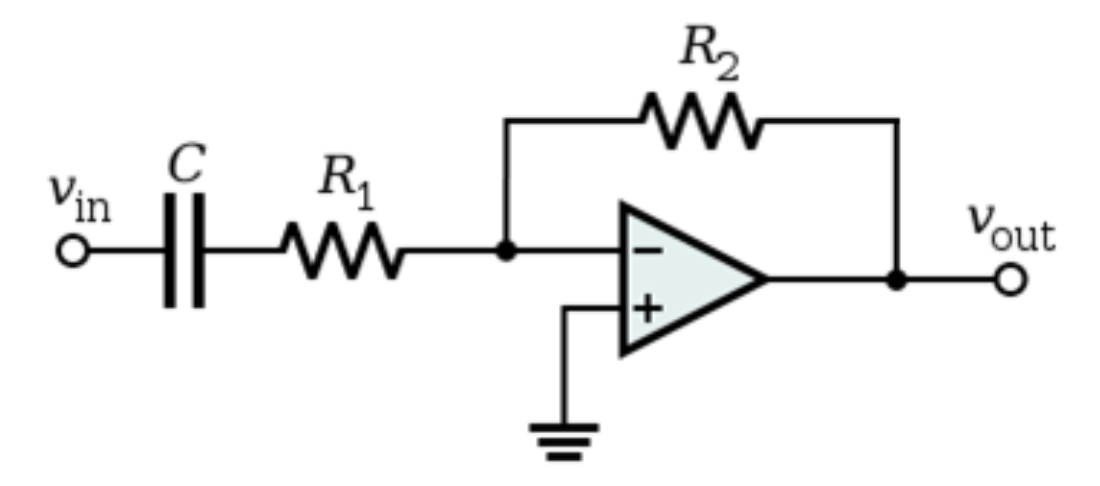 Figure 4.12: Active $1^{st}$ order high-pass filter circuit
This is an inverting amplifier with negative feedback with the addition of a capacitor. First analyse this circuit at DC where the capacitor becomes an open circuit. If the capacitor is an open circuit and the voltage at the non-inverting input is zero, the output will be zero.
Then analyse this circuit at very high frequencies where the capacitor becomes a short circuit. This is then a standard inverting op-amp and $V_{out} = - \frac{R_{2}}{R_{1}}V_{in}$ at high frequencies.
Clearly for a frequency increase from DC to high, the capacitor will allow varying amounts of current to flow, increasing the gain as the frequency increases.
The transfer can be calculated with the short-cut method:
$0 = V_{in}{[}1/(R_{1}+1/sC){]} + V_{out}(1/R_{2})$
$$\Rightarrow \frac{V_{out}}{V_{in}} = - \frac{R_{2}}{R_{1} + \frac{1}{sC}} = - \frac{sR_{2}C}{sR_{1}C + 1} = \frac{K\tau s}{\tau s + 1} = \frac{Ks}{s + \omega}$$
This is a $1^{st}$ order high-pass filter with time constant $\tau = R_{1}C$ and high frequency gain $K = - \frac{R_{2}}{R_{1}}$.
$\omega$ is again equal to $1/\tau$ and is called the cut-off frequency in rad/s.
$\frac{\mathbf{Ks}}{\mathbf{s + \omega}}$ is the form of a $1^{st}$ order high-pass filter with a high frequency gain of $K$.
Check:
$$\left.\frac{V_{out}}{V_{in}}\right|_{s = 0} = 0 \quad \checkmark$$
$$\left.\frac{V_{out}}{V_{in}}\right|_{s \to \infty} \to - \frac{R_2}{R_1} \quad \checkmark$$
Many other examples like $2^{nd}$ order high-pass filters, notch filters, band-pass filters and higher order filters can be analysed.
Active band-pass filter
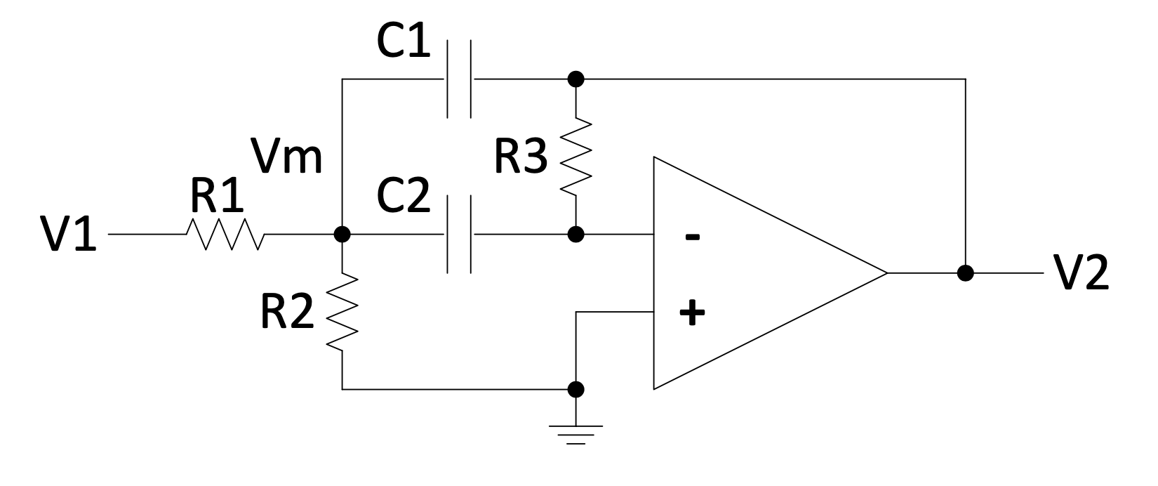 Figure 4.13: Active band-pass filter circuit
Can you see that the gains at very low and very high frequencies will approach zero?
Apply the short-cut method:
$V_{m}(1/R_{1} + 1/R_{2} + sC_{1} + sC_{2}) = V_{1}(1/R_{1}) + V_{2}(sC_{1})$; and
$0 = V_{m}(sC_{2}) + V_{2}(1/R_{3})$
Get rid of $V_{m}$:
$- \frac{V_{out}}{sR_{3}C_{2}}\left\lbrack \frac{1}{R_{1}} + \frac{1}{R_{2}} + s\left( C_{1} + C_{2} \right) \right\rbrack - V_{out}sC_{1} = V_{in}/R_{1}$
Multiply all terms with $sR_{1}R_{2}R_{3}C_{2}$:
$- V_{out}\left\lbrack R_{2} + R_{1} + sR_{1}R_{2}\left( C_{1} + C_{2} \right) + s^{2}R_{1}R_{2}R_{3}C_{1}C_{2} \right\rbrack = V_{in}sR_{2}R_{3}C_{2}$
$$\Rightarrow \frac{V_{out}}{V_{in}} = \frac{- s\frac{1}{R_{1}C_{1}}}{s^{2} + s\frac{C_{1} + C_{2}}{R_{3}C_{1}C_{2}} + \frac{R_{1} + R_{2}}{R_{1}R_{2}R_{3}C_{1}C_{2}}} = \frac{2\zeta\omega_n Ks}{s^{2} + 2\zeta\omega_n s + \omega_n^{2}}$$
This is a band-pass filter, with resonance frequency $\omega_n = \sqrt{\frac{R_{1} + R_{2}}{R_{1}R_{2}R_{3}C_{1}C_{2}}}$ in rad/s and damping $\zeta$.
The damping will determine the width of the passing band.
$K$ is the gain at frequency $\omega_n$ and can be proven to be so by substituting s = i$\omega_n$ in the last equation.
$\frac{\mathbf{2}\mathbf{\zeta\omega_n Ks}}{\mathbf{s}^{\mathbf{2}}\mathbf{+ 2}\mathbf{\zeta\omega_n s +}\mathbf{\omega_n}^{\mathbf{2}}}$ is the form of a $2^{nd}$ order band-pass filter with gain K at frequency ωn.
Check:
$$\left.\frac{V_{2}}{V_{1}}\right|_{s = 0} = 0 \quad \checkmark$$
$$\left.\frac{V_{2}}{V_{1}}\right|_{s \to \infty} \to 0 \quad \checkmark$$
$$\left.\frac{V_{2}}{V_{1}}\right|_{s = i\omega} = - \frac{R_3C_2}{R_1\left( C_1 + C_2 \right)} \quad \checkmark$$
and this can be proven to be equal to the K defined above.
The Bode plot of a band-pass filter is shown below, for various values of $\zeta$ and cut-off frequencies:
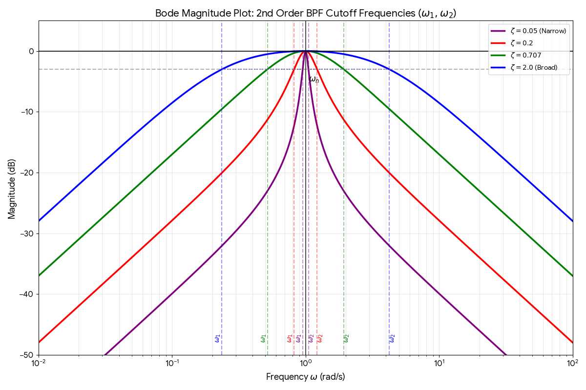 Figure 4.14: Bode plot of a band-pass filter
Example 4.2
$$\frac{V_{2}}{V_{1}} = \frac{- s\frac{1}{R1C1}}{s^{2} + s\frac{C1 + C2}{R3C1C2} + \frac{R1 + R2}{R1R2R3C1C2}} = \frac{2\zeta\omega_n Ks}{s^{2} + 2\zeta\omega_n s + \omega_n^{2}}$$
Specifications: Centre frequency of 70 Hz, $\omega_n = 2\pi \times 70 = 439.8$ rad/s
Damping $\zeta = 0.5$
Gain $K = -3.5$
There are 5 unknowns (components $R_{1}$, $R_{2}$, $R_{3}$, $C_{1}$ and $C_{2}$), 3 equations, therefore 2 components can be chosen and the remaining 3 components can be calculated and selected from the E12 series.
A set of design results is: $R_{1} = R_{2} = 10 k\Omega$
$R_{3} = 43 k\Omega$, $C_{1} = 68 nF$, $C_{2} = 0.39 \mu F$
Check:
Resulting design parameters, following from the equations above:
$\omega_n = \sqrt{\frac{R_{1} + R_{2}}{R_{1}R_{2}R_{3}C_{1}C_{2}}} = 2\pi \times 66.65$ rad/s,
$\zeta = \frac{\frac{C_{1} + C_{2}}{R_{3}C_{1}C_{2}}}{2\omega_n} = 0.48$, with $\omega_n = 2\pi \times 66.65$ rad/s and
$K = - \frac{\frac{1}{R_{1}C_{1}}}{2\zeta\omega_n} = - 3.66$, with $\zeta = 0.48$ and $\omega_n = 2\pi \times 66.65$ rad/s
Because of the particular 3 equations, the design parameters must be determined in this specific sequence, because $\omega_n$ is only dependent on the component values, then $\zeta$ is only dependent on this calculated $\omega_n$ and components, and then $K$ is dependent on these calculated $\omega_n$ and $\zeta$ and components.
[% errors]{.underline} (check the signs!):
$\% \omega_n$ error $= \frac{66.65 - 70}{70} \times 100\% = - 4.8\%$
$\% \zeta$ error $= \frac{0.48 - 0.5}{0.5} \times 100\% = - 4.0\%$
$\% K$ error $= \frac{- 3.66 - ( - 3.5)}{- 3.5} \times 100\% = + 4.6\%$
Here is a $2^{nd}$ example of a band-pass filter.
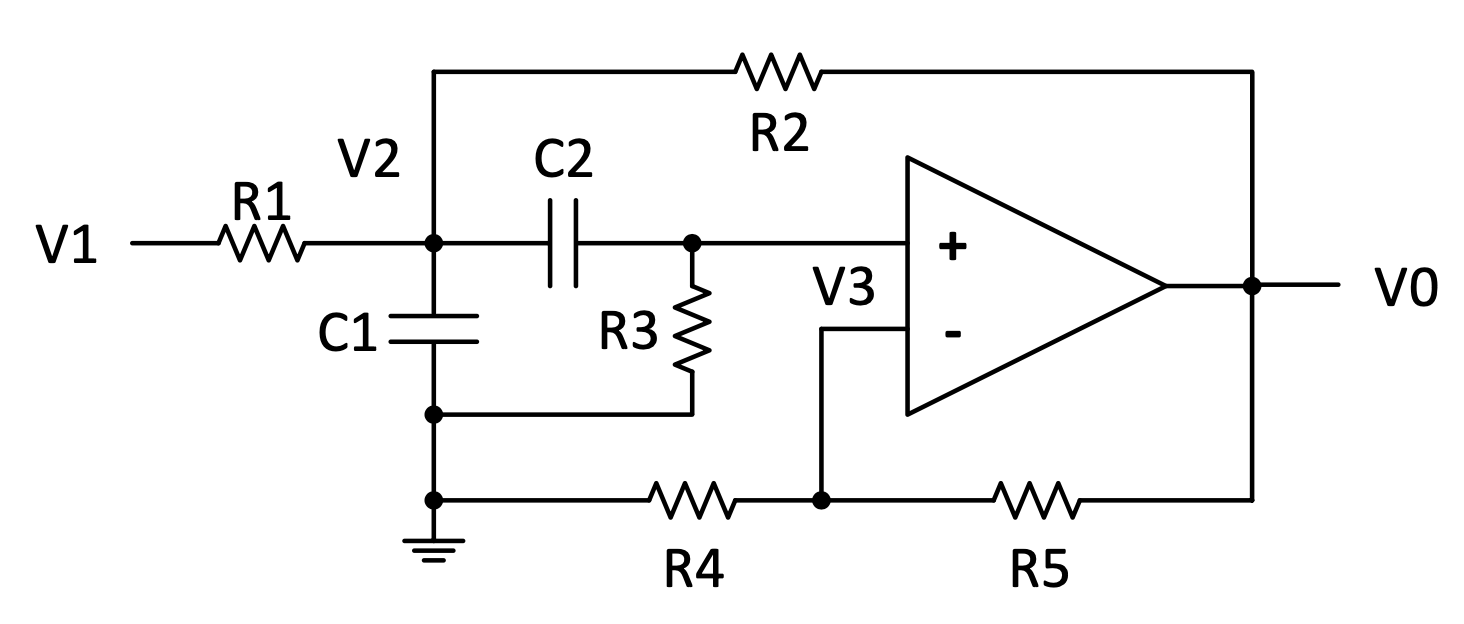 Figure 4.15: Another active band-pass filter circuit
Question 4.1
Derive the transfer function of the circuit in Figure 4.15:
$\frac{V_{0}}{V_{1}}(s) = \frac{s\frac{1}{C_{1}R_{1}}\left( 1 + \frac{R_{5}}{R_{4}} \right)}{s^{2} + s\left\lbrack \frac{1}{R_{3}}\left( \frac{1}{C_{1}} + \frac{1}{C_{2}} \right) + \frac{1}{C_{1}}\left( \frac{1}{R_{1}} - \frac{R_{5}}{R_{2}R_{4}} \right) \right\rbrack + \frac{1}{C_{1}C_{2}R_{3}}\left( \frac{1}{R_{1}} + \frac{1}{R_{2}} \right)}$
Notch filters
The above filters are useful if you have wide band noise. However sometimes you need to eliminate a specific frequency such as 50 Hz. For this you can use a notch filter.
Active notch filter:
This can be realized by adding the outputs of a low-pass and high-pass filter.
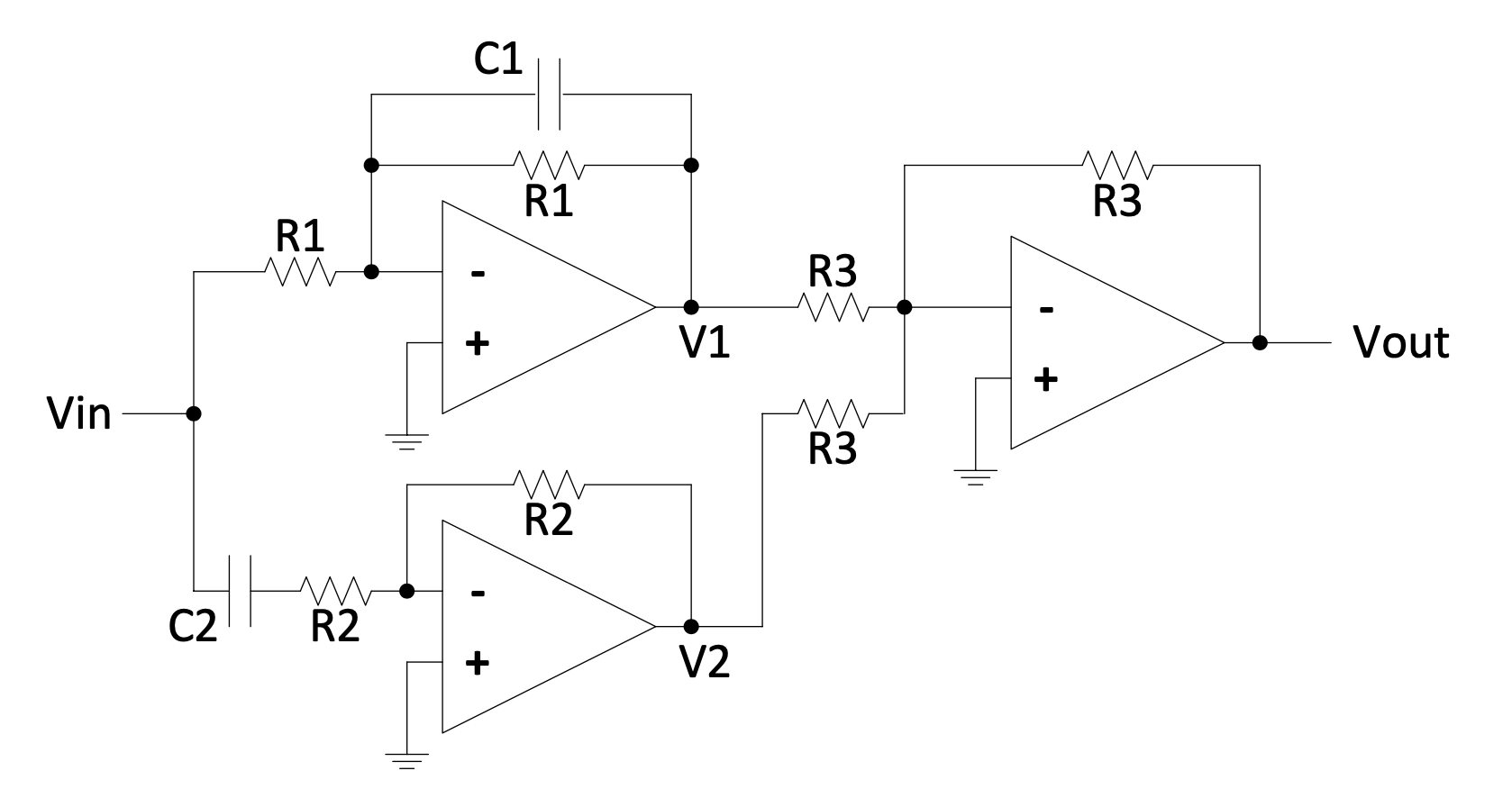 Figure 4.16: Active notch filter circuit
From the equations for the active $1^{st}$ order low-pass and high-pass filters follow:
$V_{1} = - \frac{\frac{1}{R_{1}C_{1}}}{s + \frac{1}{R_{1}C_{1}}}V_{in}$
$V_{2} = - \frac{s}{s + \frac{1}{R_{2}C_{2}}}V_{in}$
$V_{out} = - \left( V_{1} + V_{2} \right)$
$\therefore V_{out} = \frac{R_{3}}{R_{3}}\left( \frac{\frac{1}{R_{1}C_{1}}}{s + \frac{1}{R_{1}C_{1}}} + \frac{s}{s + \frac{1}{R_{2}C_{2}}} \right)V_{in} = \frac{\frac{1}{R_{1}C_{1}}\left( s + \frac{1}{R_{2}C_{2}} \right) + s\left( s + \frac{1}{R_{1}C_{1}} \right)}{\left( s + \frac{1}{R_{1}C_{1}} \right)\left( s + \frac{1}{R_{2}C_{2}} \right)}V_{in} = \frac{s^{2} + \left( \frac{2}{R_{1}C_{1}} \right)s + \frac{1}{R_{1}C_{1}R_{2}C_{2}}}{s^{2} + \left( \frac{1}{R_{1}C_{1}} + \frac{1}{R_{2}C_{2}} \right)s + \frac{1}{R_{1}C_{1}R_{2}C_{2}}}V_{in}$
$$\Rightarrow\frac{V_{out}}{V_{in}} = \frac{s^{2} + \left( \frac{2}{R_{1}C_{1}} \right)s + \frac{1}{R_{1}C_{1}R_{2}C_{2}}}{s^{2} + \left( \frac{1}{R_{1}C_{1}} + \frac{1}{R_{2}C_{2}} \right)s + \frac{1}{R_{1}C_{1}R_{2}C_{2}}} = \frac{s^{2} + 2\zeta_{1}\omega_n s + \omega_n^{2}}{s^{2} + 2\zeta_{2}\omega_n s + \omega_n^{2}}$$
$\mathbf{\frac{s^{2} + 2\zeta_{1}\omega_n s + \omega_n^{2}}{s^{2} + 2\zeta_{2}\omega_n s + \omega_n^{2}}}$ is the form of a $2^{nd}$ order notch filter with DC and high frequency gain of 1.
The gains are:
-
At low frequency: 1.0
-
At notch frequency: $\frac{\zeta_{1}}{\zeta_{2}} = \frac{\frac{2}{R_{1}C_{1}}}{\frac{1}{R_{1}C_{1}} + \frac{1}{R_{2}C_{2}}}$
-
At high frequency: 1.0
The notch frequency is at the natural frequency: $\omega_n = \sqrt{\frac{1}{R_{1}C_{1}R_{2}C_{2}}}$, in rad/s.
The Bode plot of a notch filter is shown below.
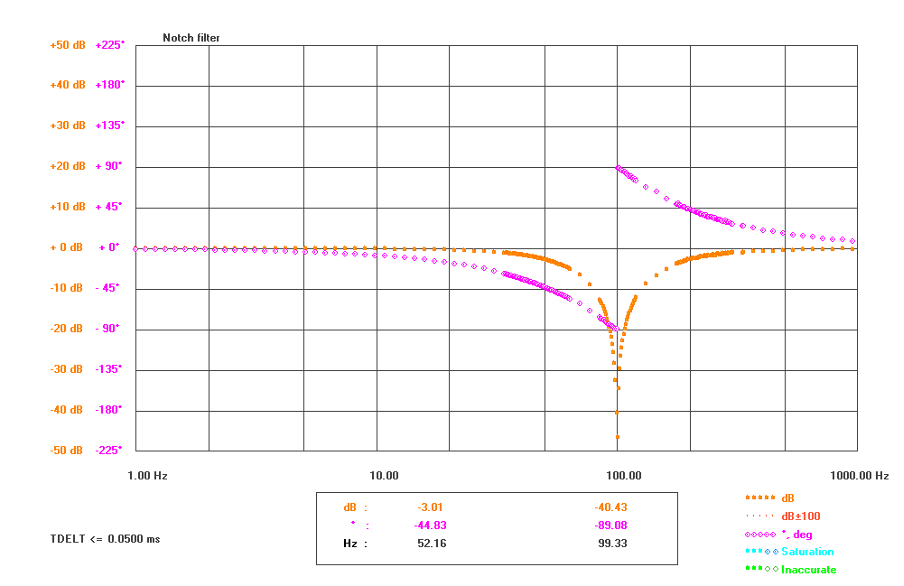 Figure 4.17: Bode plot of a notch filter
Question 4.2
What would you change to add some gain to this active notch filter?
Example 4.3
$$\frac{V_{out}}{V_{in}} = \frac{s^{2} + \left( \frac{2}{R_{1}C_{1}} \right)s + \frac{1}{R_{1}C_{1}R_{2}C_{2}}}{s^{2} + \left( \frac{1}{R_{1}C_{1}} + \frac{1}{R_{2}C_{2}} \right)s + \frac{1}{R_{1}C_{1}R_{2}C_{2}}} = \frac{s^{2} + 2\zeta_{1}\omega_n s + \omega_n^{2}}{s^{2} + 2\zeta_{2}\omega_n s + \omega_n^{2}}$$
With $\zeta_{1}$, $\zeta_{2}$ and $\omega_n$ specified, there are 4 unknowns (components $R_{1}$, $R_{2}$, $C_{1}$ and $C_{2}$), 3 equations, therefore one would think that 1 component can be chosen and the remaining 3 components can be calculated and selected (from the E12 series). However, in this case, the $\frac{\zeta_{1}}{\zeta_{2}}$ ratio can be specified, or any one of $\zeta_{1}$ or $\zeta_{2}$ but not both. One has to work through this example to see this.
Question 4.3
You may try the following specifications:
$\frac{\zeta_{1}}{\zeta_{2}} = 0.01$ and $\omega_n = 160$ rad/s
This type of restriction on specifications is not unique to some notch filters, but can also occur with other filters depending on their implementation configuration.
A notch filter can also be realized by subtracting a band-pass filter’s transfer function from a gain. The following circuit will do this:
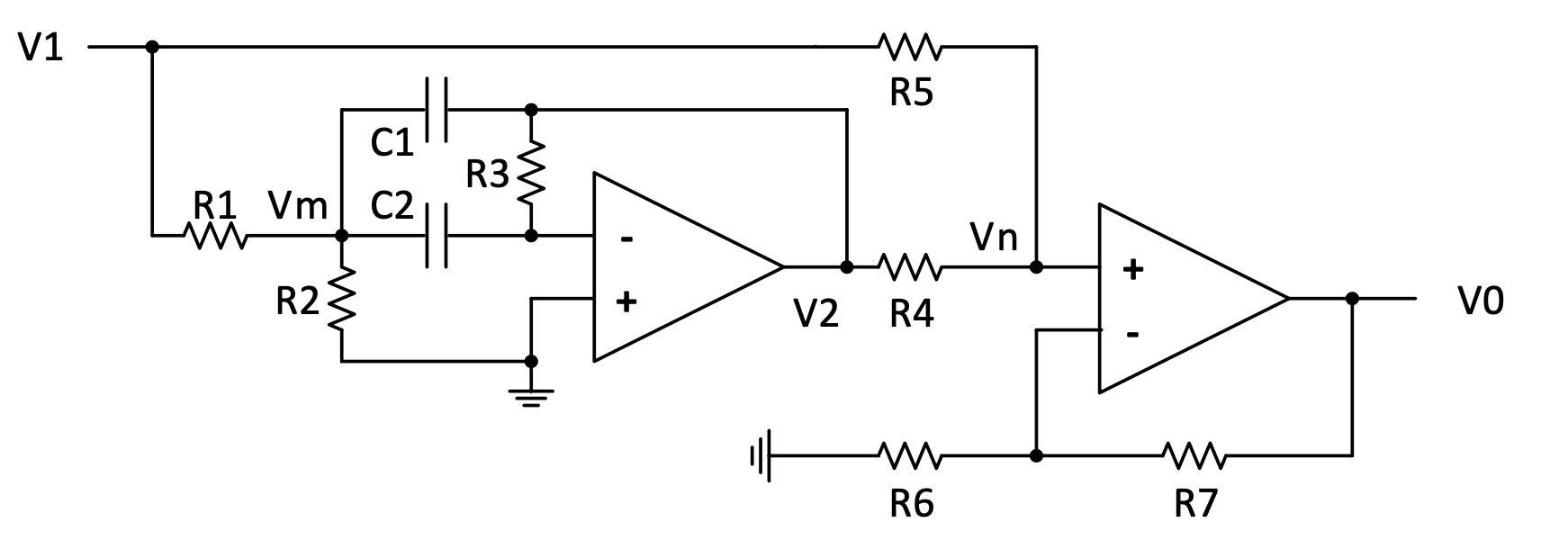 Figure 4.18: Active notch filter circuit formed by subtracting a band-pass filter’s transfer function from a gain
The transfer function is: $\frac{V_{0}}{V_{1}} = \frac{1 + \frac{R_{7}}{R_{6}}}{1 + \frac{R_{5}}{R_{4}}} . \frac{s^{2} + \left\lbrack \frac{1}{R_{3}}\left( \frac{1}{C_{1}} + \frac{1}{C_{2}} \right) - \frac{R_{5}}{R_{4}} . \frac{1}{R_{1}C_{1}} \right\rbrack s + \frac{1}{R_{3}C_{1}C_{2}}\left( \frac{1}{R_{1}} + \frac{1}{R_{2}} \right)}{s^{2} + \frac{1}{R_{3}}\left( \frac{1}{C_{1}} + \frac{1}{C_{2}} \right)s + \frac{1}{R_{3}C_{1}C_{2}}\left( \frac{1}{R_{1}} + \frac{1}{R_{2}} \right)} = K\frac{s^{2} + 2\zeta_{1}\omega_n s + \omega_n^{2}}{s^{2} + 2\zeta_{2}\omega_n s + \omega_n^{2}}$
It was derived by first getting $\frac{V_{2}}{V_{1}}(s)$, similar to what was done before because this part is a band-pass filter. Next, the two short-cut method equations can be written down for $V_{n}$. From these 3 equations, by doing the algebra carefully, $\frac{V_{0}}{V_{1}}(s)$, can be found.
Example 4.4
In this case, all parameters can be specified, for example:
$K = 1$, $\zeta_{1} = 0.01$, $\zeta_{2} = 1.0$ and $\omega_n = 160$ rad/s.
From $\omega_n^{2} = \frac{1}{R_{3}C_{1}C_{2}}\left( \frac{1}{R_{1}} + \frac{1}{R_{2}} \right)$, choosing $R_{1} = R_{2} = 10k$ follows: $R_{3}C_{1}C_{2} = 7.8125e-9$.
Note that $2\zeta_{2}\omega_n = \frac{C_{1} + C_{2}}{R_{3}C_{1}C_{2}}$, thus $C_{1} + C_{2} = 2.5e-6$.
This can be realized with 1.0 $\mu$F and 1.5 $\mu$F capacitors, but smaller capacitors would be better. Choose therefore $R_{1} = R_{2} = 100k$, therefore $R_{3}C_{1}C_{2} = 7.8125e-10$, therefore $C_{1} + C_{2} = 2.5e-7$.
Let $C_{1} = 0.1 \mu F$, therefore $C_2 = 0.15 \ \mu F$, therefore $R_{3} = 51k + 1k$.
$\frac{1}{R_{3}}\left( \frac{1}{C_{1}} + \frac{1}{C_{2}} \right) - \frac{R_{5}}{R_{4}} . \frac{1}{R_{1}C_{1}} = 2\zeta_{2}\omega_n$, therefore $\frac{R_{5}}{R_{4}} = 3.173$.
Let $R_{4} = 47k$, therefore $R_{5} = 150k$.
$K = \frac{1 + \frac{R_{7}}{R_{6}}}{1 + \frac{R_{5}}{R_{4}}} = 1.0$, therefore $\frac{R_{7}}{R_{6}} = 3.191$.
$\frac{1}{R_{3}}\left( \frac{1}{C_{1}} + \frac{1}{C_{2}} \right) - \frac{R_{5}}{R_{4}} . \frac{1}{R_{1}C_{1}} = 2\zeta_{2}\omega_n$, therefore $\frac{R_{5}}{R_{4}} = 3.173$.
Let $R_{4} = 47k$, therefore $R_{5} = 150k$.
Let $R_{6} = 16k$, therefore $R_{7} = 51k$.
Compensator networks
Compensators are used in control loop designs. How to design their time constant values, is not covered in this course, but how to implement them, and design the components to produce the time constants, are done in this section.
In general, a compensator is of the form: $k\frac{\tau_{1}s + 1}{\tau_{2}s + 1}$, with k a gain, $\tau_{1}$ the lead time constant, and $\tau_{2}$ the lag time constant.
It can be implemented with either of the following circuits, the first producing a negative gain, and the second not.
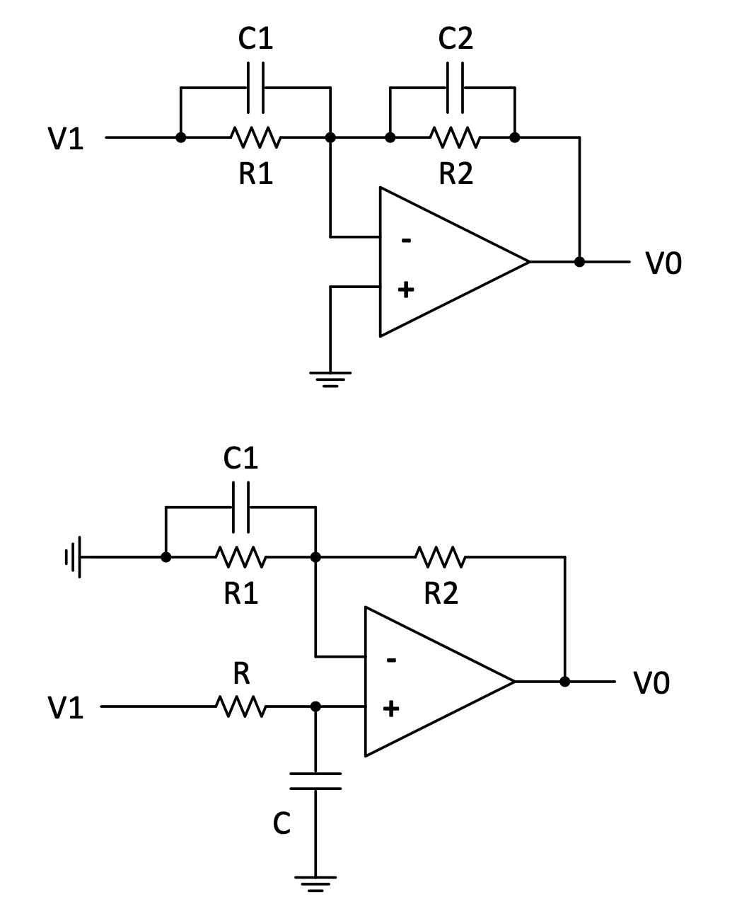 Figure 4.19: Compensator networks
Question 4.4
Calculate the transfer functions $\frac{V_{0}}{V_{1}}$ for the two circuits above.
The answers are: $- \frac{R_{2}}{R_{1}} . \frac{sC_{1}R_{1} + 1}{sC_{2}R_{2} + 1}$ and $\left( 1 + \frac{R_{2}}{R_{1}} \right)\frac{s\frac{C_{1}R_{1}R_{2}}{R_{1} + R_{2}} + 1}{sCR + 1}$
Summary of transfer functions of filters
In general, $\tau$ refers to the time constant (in s) associated with the filter, $\omega_c$ with the cut-off frequency (in rad/s) of the filter, $\omega_n$ with the natural frequency (in rad/s) of the filter, $\zeta$ with the damping factor, and $K$ with some gain in the filter.
Low-pass filter, $1^{st}$ order:
$\frac{V_{out}}{V_{in}} = \frac{K}{\tau s + 1} = \frac{K\omega_c}{s + \omega_c}$
High-pass filter, $1^{st}$ order:
$\frac{V_{out}}{V_{in}} = \frac{K\tau s}{\tau s + 1} = \frac{Ks}{s + \omega_c}$
Low-pass filter, $2^{nd}$ order:
$\frac{V_{out}}{V_{in}} = \frac{K\omega_n^{2}}{s^{2} + 2\zeta\omega_n s + \omega_n^{2}}$
High-pass filter, $2^{nd}$ order:
$\frac{V_{out}}{V_{in}} = \frac{Ks^{2}}{s^{2} + 2\zeta\omega_n s + \omega_n^{2}}$
Band-pass filter, $2^{nd}$ order:
$\frac{V_{out}}{V_{in}} = K\frac{2\zeta\omega_n s}{s^{2} + 2\zeta\omega_n s + \omega_n^{2}}$
Notch filter, $2^{nd}$ order:
$\frac{V_{out}}{V_{in}} = K\frac{s^{2} + 2\zeta_{1}\omega_n s + \omega_n^{2}}{s^{2} + 2\zeta_{2}\omega_n s + \omega_n^{2}}$
The gain at a particular frequency, $\omega$, can be determined by replacing s with $j\omega$.
Therefore, the gain at $\omega$ will e.g. be:
-
K for the $2^{nd}$ order band-pass filter
-
$K\frac{\zeta_{1}}{\zeta_{2}}$ for the notch filter
Example solutions
Solutions to the examples in this section can be found here.