Analog-to-Digital Conversion
Table of Contents
Analogue-to-Digital Converters (ADCs) are devices that are used to convert continuous analogue signals into discrete digital values. This chapter covers the fundamentals of ADC operation and implementation on STM32 microcontrollers.
The lecture slides used for this section are available here.
Introduction to ADC
The ADC peripheral in STM32 microcontrollers provides a bridge between the analogue and digital domains, enabling the microcontroller to process real-world signals. Key features include:
- Up to 12-bit resolution ADC. On the STM32F0 the resolution is selectable to 6, 8, 10, or 12 bits.
- 19 sample channels (16 external, 3 internal).
- Single converter with multiplexed inputs.
- Configurable conversion parameters.
- Hardware triggers and DMA support.
These, and further features are described in Section 13.2 of the STM32F0 Reference Manual:
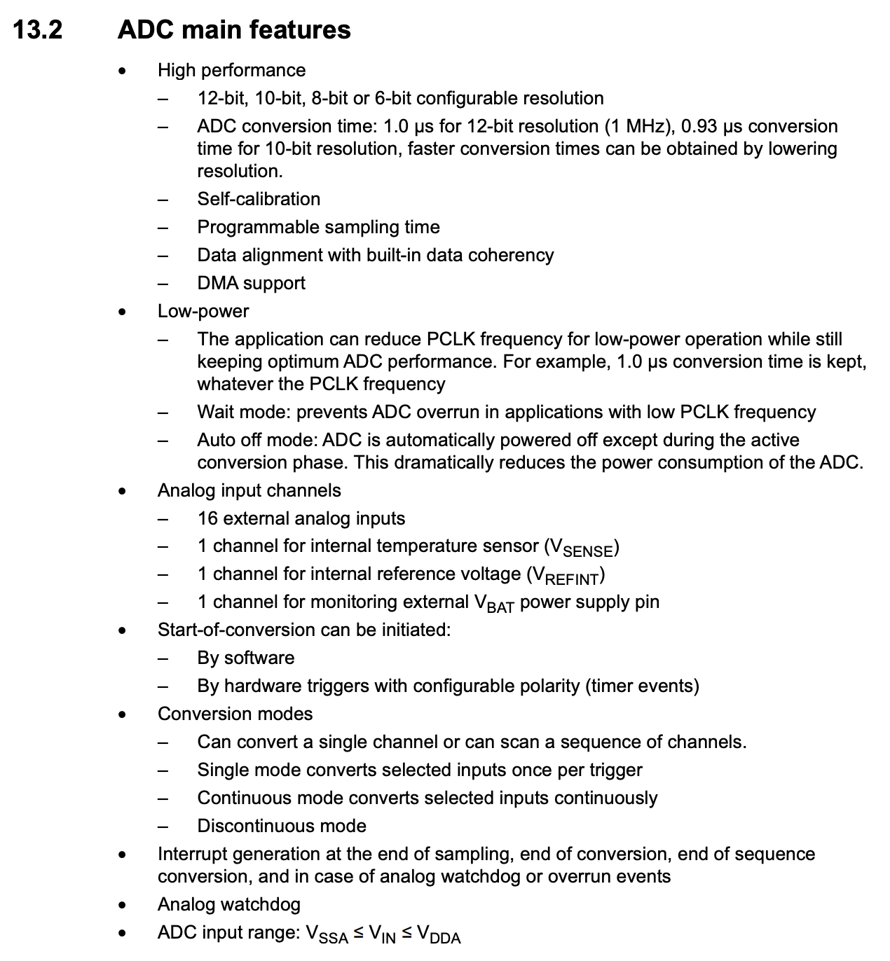 Figure 8.1: Features of the ADC on the STM32F0 [1]
The governing equation for an ADC is shown in the equation below:
$$\text{ADC value} = \lfloor \frac{V_{in}}{V_{max}} \times (2^{n}-1) \rfloor$$
On the STM32, it is helpful to distinguish between the main microcontroller supply and the ADC reference supply. The MCU core is powered from V_DD, whilst the ADC conversion range is determined by V_DDA. In many simple laboratory setups these are both 3.3 V, which is why it is common to take $V_{max} = 3.3\text{ V}$ in examples.
Where:
- $V_{in}$ is the input voltage.
- $V_{max}$ is the ADC maximum voltage (3.3V for an STM32).
- $n$ is the ADC resolution, a value you set in firmware.
- $\lfloor * \rfloor$ means rounding down to the next closest integer value.
So say we have an input signal of 1.23V, the ADC max voltage is 3.3V and the resolution is 10 bits. That would results in a value of:
$$ \text{ADC value} = \lfloor \frac{1.23}{3.3} \times (2^{10}-1) \rfloor = 381 $$
That value is about a third of $2^{10}$, which should make sense as $V_{in}$ was about a third of $V_{max}$.
ADC Architecture
The block diagram below, taken from the lecture slides, is a useful high-level view of the ADC peripheral. It shows that the ADC is not only the converter itself, but also includes input channel selection, start/stop control, sampling-time configuration, the conversion core, and the interfaces used to raise interrupts or DMA requests.
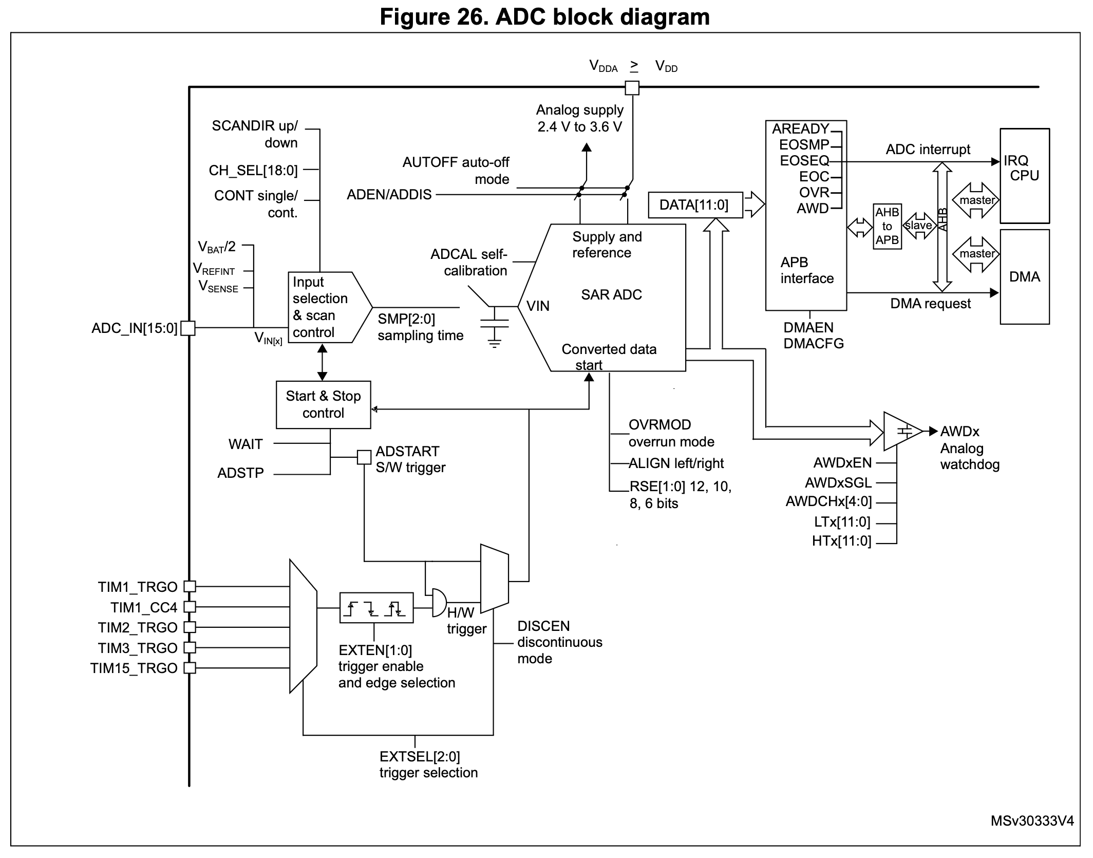 Figure 8.2: High-level ADC block diagram from STM32F0 Reference Manual [1]
Input Channels
The ADC supports multiple input channels:
- 16 external channels (ADC_IN[15:0]) - these are routed from the GPIO pins when configured in Analogue mode.
- 3 internal channels:
- V_BAT (battery voltage).
- V_REF (reference voltage).
- TS (temperature sensor).
Conversion Modes
The ADC can operate in different modes, however, unless it is configured in the rarely used Discontinuous mode (set by then DISCEN) bit, the ADC always converts a sequence of channels once triggered:
- Single conversion - here the selected channels are converted, in sequence of their selection, once before the ADC stops conversions. This behaviour is described in 13.3.8 of the Reference Manual:
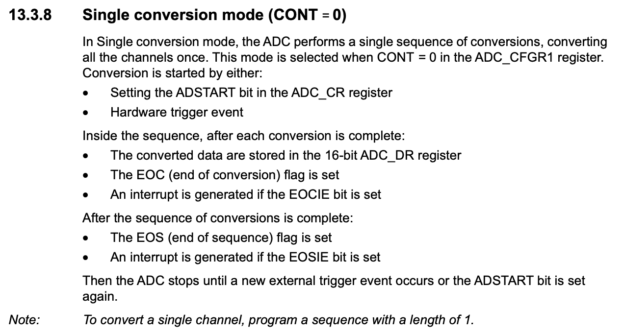 Figure 8.2: Functional description of the single conversion mode of the ADC [1]
- Continuous conversion - here the selected channels are converted, in sequence of their selection, and once the sequence is complete, it is begun again until the ADC is either stopped or disabled. This behaviour is described in 13.3.9 of the Reference Manual:
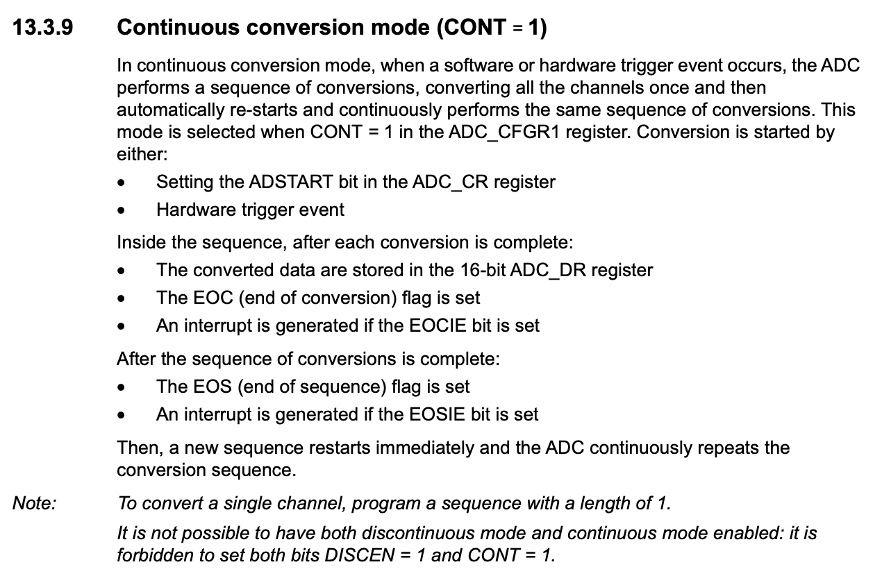 Figure 8.3: Functional description of the continuous conversion mode of the ADC [1]
Within these modes, an Up scan is defined as from ADC_IN0 first, whilst a Down scan is from VBAT first.
Conversion Start and Stop
The ADC must be told when to begin a conversion sequence. This can be done in software by setting the ADSTART bit in ADC_CR, or by using one of the available hardware trigger sources. In simple applications, software triggering is the most common approach because it gives direct control over when a conversion begins.
Likewise, conversion is not only about starting. The ADC also provides control over stopping a conversion sequence when needed. In practice, the programmer should think of the ADC as a peripheral which must be configured, started, monitored while it works, and then either retriggered or stopped depending on the operating mode being used.
ADC Configuration
Enabling the ADC
As with all peripherals on the microcontroller, the ADC peripheral must be enabled before it can be used. This is done by enabling the ADC clock in the RCC_APB2ENR register:
RCC->APB2ENR |= RCC_APB2ENR_ADCEN;
Once the clock is enabled, the ADC peripheral must be activated by setting the ADEN bit in the ADC_CR register:
ADC1->CR |= ADC_CR_ADEN;
On the STM32F0, care must be taken in order of enabling and configuring the ADC peripheral. These details can be found in the instructions of Section 13.3.5 of the Reference Manual:
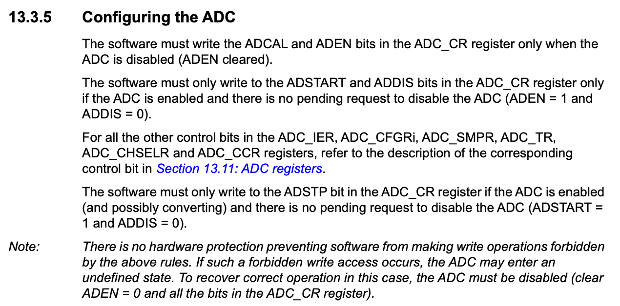 Figure 8.4: Order of enabling and configuring the ADC peripheral [1]
Channel Selection
Channel selection is done by configuring the GPIO pins for analogue mode and then selecting the channels in the ADC_CHSELR register. This can be seen in the instructions of Section 13.3.6 of the Reference Manual:
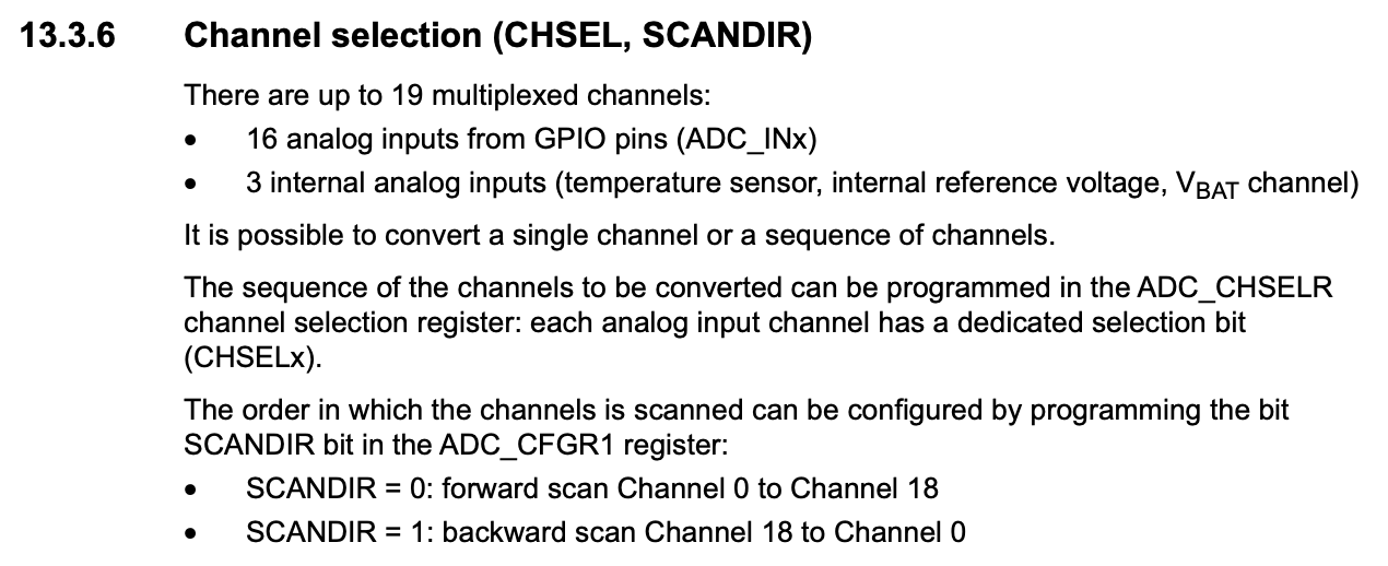 Figure 8.5: Channel selection in the ADC [1]
For example, to configure and select GPIOA6 as an ADC channel:
Although the ADC peripheral supports up to 16 external input channels, the specific STM32 package used in a design may expose only a subset of those channels on physical pins. For this reason, it is important to check the datasheet rather than assume that every ADC input is available. For example, on the STM32F0 used in this course, PA5 is connected to ADC channel 5 and PA6 is connected to ADC channel 6.
- Configure GPIO pins for analogue input:
GPIOA->MODER |= GPIO_MODER_MODER6; // Example for PA6 - Select channels in the ADC_CHSELR register which correspond to the configured GPIO:
ADC1->CHSELR |= ADC_CHSELR_CHSEL; // Example for channel 6
Resolution and Alignment
The ADC supports configurable resolution and data alignment. Lower resolutions result in faster conversions, but with a loss of precision. The resolution and alignment can be set in the ADC_CFGR1 register.
In practice, this means there is a trade-off between precision and speed. If an application does not require the full 12-bit resolution, the ADC should be configured for 10-bit, 8-bit, or 6-bit conversions instead. This reduces the amount of information captured in each sample, but allows the ADC to complete conversions more quickly.
- Default 12-bit resolution
- Option for 8-bit resolution:
ADC1->CFGR1 |= ADC_CFGR1_RES_1;
The ADC data register (ADC_DR) is the register where the ADC conversion result is stored. It is 32 bits wide and the most significant 16 bits are not used. The ADC output is a maximum of 12 bits wide and is governed by the chosen resolution, thus, not all bits are used for storing data in the ADC_DR register. The data is then be right or left justified, accordingly:
Right Justified (ALIGN = 0): ADC_DR[15:0] = [0 0 0 b12 b11 b10 b9 b8 b7 b6 b5 b4 b3 b2 b1 b0]
Left Justified (ALIGN = 1): ADC_DR[15:0] = [b12 b11 b10 b9 b8 b7 b6 b5 b4 b3 b2 b1 b0 0 0 0]
- Data alignment (right or left):
ADC1->CFGR1 |= ADC_CFGR1_ALIGN; // Left alignment
Wait mode
The ADC can be configured to use a low power mode by the setting of the WAIT bit in the ADC_CFGR1 register. This causes the ADC to pause in its sequence of conversions until the ADC_DR register is read. This can be seen in the instructions of Section 13.6 of the Reference Manual:
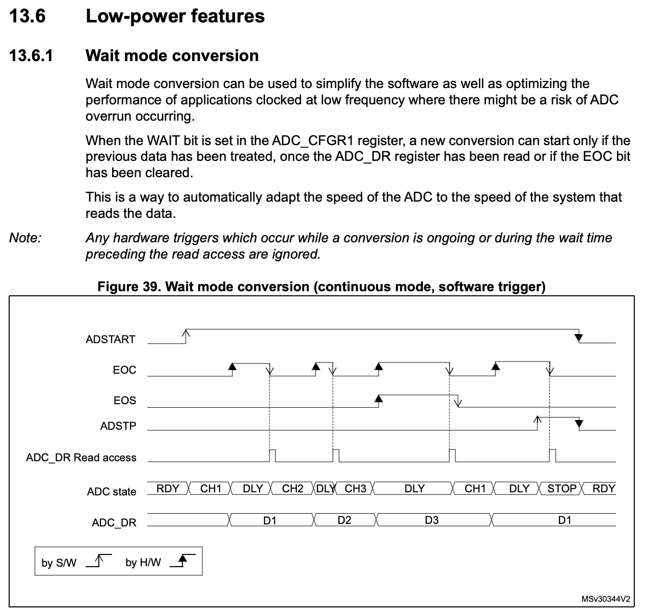 Figure 8.6: Wait mode in the ADC [1]
In addition to lowering the power usaage of the ADC (becuase conversions are not continually being performed), this setting has the additional benefit of preventing data loss by forcing each conversion to be read before the next one begins.
Conversion Monitoring
Once enabled, the ADC takes some time to complete its configuration and may only be used once the ADC Ready flag is raised in the Interrupt and Status Register (ISR). Typically after configuration and enabling, the programmer inserts a line such as that below to wait until the ADC may be used:
while((ADC1->ISR & ADC_ISR_ADRDY) == 0); // Wait for ADC ready
Once the ADC is ready, the programmer can then trigger a conversion by setting the ADSTART bit in the ADC_CR register (if using software triggering). This can be seen in the instructions of Section 13.3.10 of the Reference Manual:
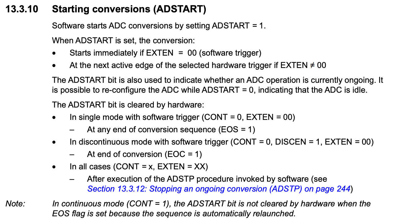 Figure 8.7: Starting a conversion in the ADC [1]
The general sequence for a single-shot conversion is:
- Start the conversion sequence by setting
ADSTARTinADC_CR, or by using a hardware trigger. - Wait for the
EOCbit inADC_ISRto go high after the conversion completes. - Read the result from
ADC_DRin the format determined by the selected resolution and alignment. - Start a new conversion later with
ADSTARTor another trigger when a new sample is required.
Once, begun, a conversion result is not instantanious. The ADC will continue to convert the selected channels until the conversion is complete. The ADC will raise the ADC_ISR_EOC flag when the conversion is complete and then raise the ADCl_ISR_EOS flag once the sequence of conversions is complete. See Figures 7.2 and 7.3 for reference. In a single conversion mode, the timings of the conversion and flag raising are as follows:
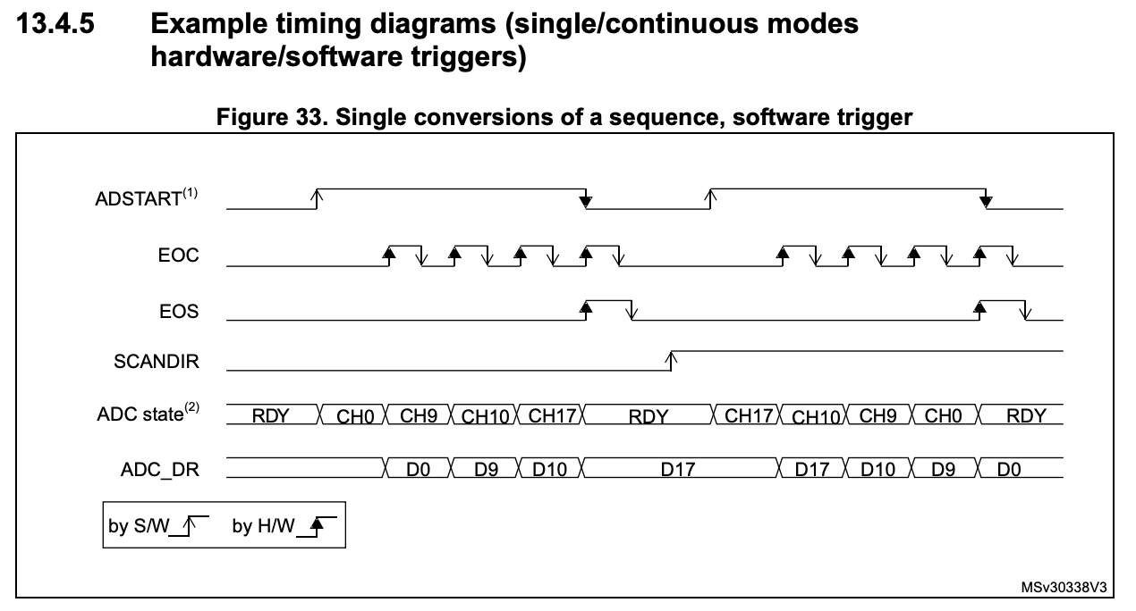 Figure 8.8: Timing of a single conversion in the ADC [1]
Conversely, in a continuous conversion mode, the timings of the conversion and flag raising are as follows:
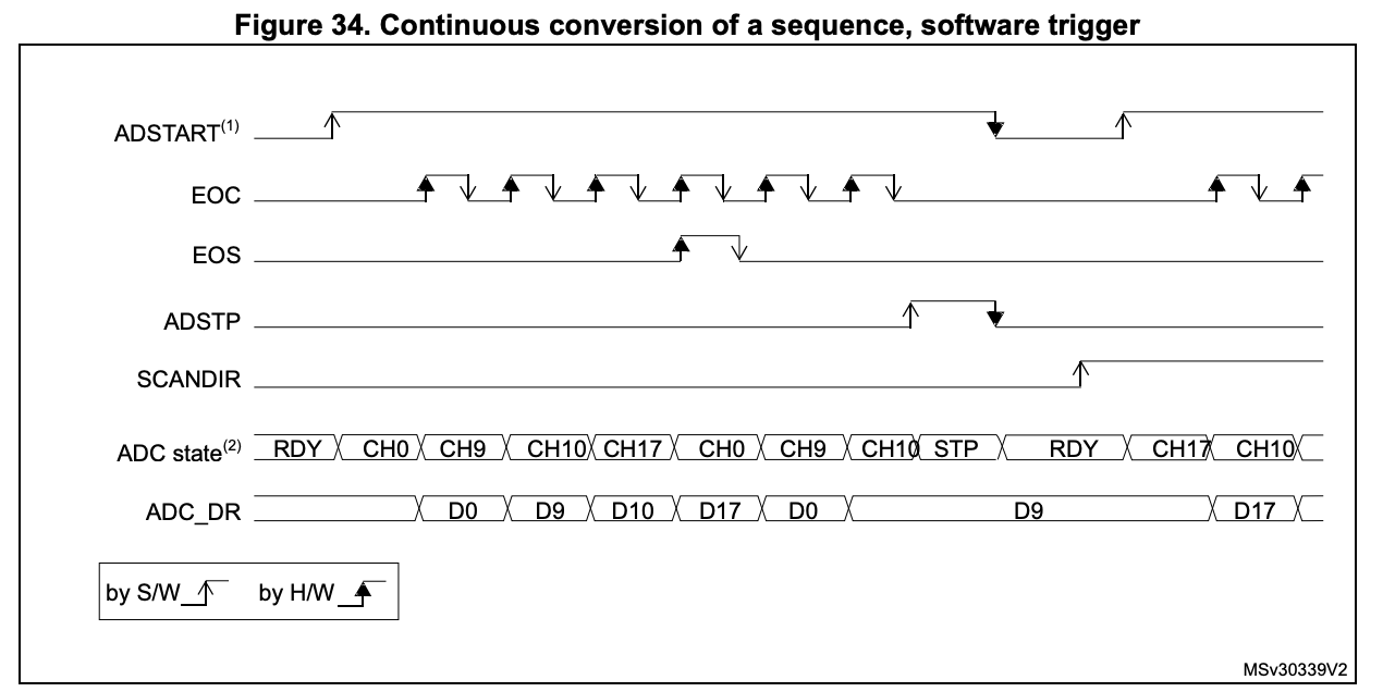 Figure 8.9: Timing of a continuous conversion in the ADC [1]
The general sequence for continuous conversion is:
- Start the conversion sequence by setting
ADSTARTinADC_CR, or by using a hardware trigger. - Wait for the
EOCbit inADC_ISRto go high after each conversion. - Read the result from
ADC_DR. - After the selected channels have been sampled, the ADC automatically begins the next sequence until conversion is stopped or the ADC is disabled.
Once the conversion of a channel is complete, the ADC_ISR_EOC flag is raised and the ADC_DR register is updated with the result. The programmer can then read the ADC_DR register to get the result of the conversion. Typically this can be done by using a while loop to wait for the ADC_ISR_EOC flag to be raised and then reading the ADC_DR register:
while((ADC1->ISR & ADC_ISR_EOC) == 0);  // Wait for conversion to complete
ADC_DR = ADC1->DR;  // Read the result
Interrupt generation
Whilst the above method is effective in simple applications, it is not ideal for more complex applications where the programmer may need to perform other tasks whilst waiting for the conversion to complete. For this reason, the ADC peripheral interrupt generation from a variety of events. Typically any flag contained in and ISR register can be used to generate an interrupt. On the STM32F0, the ADC peripheral can generate interrupts from the following events stated in Section 13.3.10 of the Reference Manual:
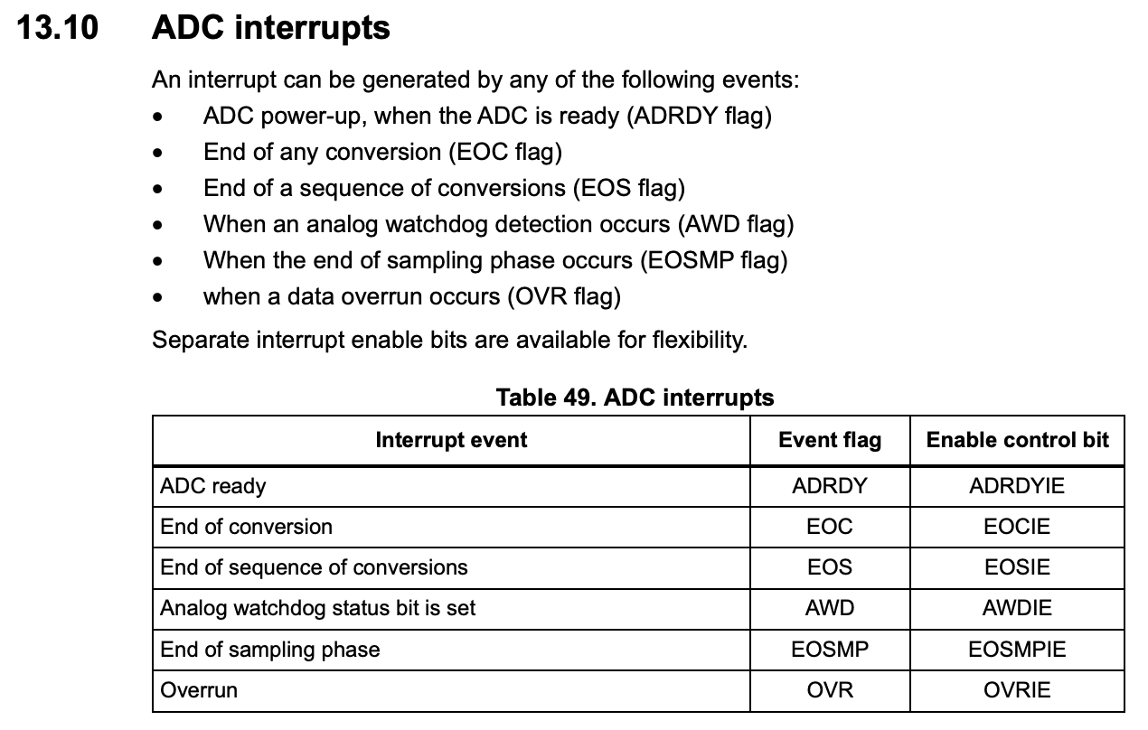 Figure 8.10: Interrupt events on the ADC [1]
Using an interrupt driven approach, the programmer can configure the ADC to raise an interrupt when a specific event occurs. For example, instead of using a while loop to wait for the conversion to complete, the programmer can configure the ADC to raise an interrupt when the conversion is complete and then handle the interrupt in the interrupt service routine. To do this, the programmer must first enable the ADC interrupt in the ADC_IER register:
ADC1->IER |= ADC_IER_EOCIE; // Enable interrupt on end of conversion
Then, the programmer must enable the ADC interrupt in the NVIC:
NVIC_EnableIRQ(ADC1_IRQn);
Finally, the programmer must implement the ADC interrupt service routine to handle the interrupt and (in this case) read the ADC_DR register:
void ADC1_COMP_IRQHandler(void)
{
    ADC_DR = ADC1->DR;  // Read the result (this action lowers the ADC_ISR_EOC flag - See description of ADC_ISR_EOC in Section 13.3.10 of the Reference Manual)
}
Worked Polling Example
The following example shows a complete polling-based ADC setup. It enables the GPIO and ADC clocks, configures PA6 as an analogue input, selects ADC channel 6, sets the ADC to 8-bit resolution, waits for the ADC to become ready, starts each conversion in software, waits for EOC, and then reads the result from ADC_DR.
#include <stdint.h>
#include "stm32f0xx.h"

static void init_adc(void);

uint16_t adc_result;

void main(void)
{
    init_adc();

    while (1)
    {
        ADC1->CR |= ADC_CR_ADSTART;              // Start conversion
        while ((ADC1->ISR & ADC_ISR_EOC) == 0);  // Wait for end of conversion
        adc_result = ADC1->DR;                   // Read result
    }
}

static void init_adc(void)
{
    RCC->AHBENR |= RCC_AHBENR_GPIOAEN;          // Enable clock for GPIOA
    RCC->APB2ENR |= RCC_APB2ENR_ADCEN;          // Enable clock for ADC

    GPIOA->MODER |= GPIO_MODER_MODER6;          // Set PA6 to analogue mode
    ADC1->CHSELR |= ADC_CHSELR_CHSEL6;          // Select ADC channel 6
    ADC1->CFGR1 |= ADC_CFGR1_RES_1;             // Set 8-bit resolution
    ADC1->CR |= ADC_CR_ADEN;                    // Enable ADC

    while ((ADC1->ISR & ADC_ISR_ADRDY) == 0);  // Wait until ADC is ready
}
The value stored in adc_result can then be used elsewhere in the program, for example to drive LEDs, make a control decision, or transmit the measurement over a communication peripheral.
References
[1] ST Microelectronics, ‘RM0091 Reference Manual’. May 2022. [Online]. Available: https://www.st.com/resource/en/reference_manual/rm0091-stm32f0x1stm32f0x2stm32f0x8-advanced-armbased-32bit-mcus-stmicroelectronics.pdf