Timer Peripherals
Table of Contents
- Timer Peripherals
Timers are hardware counters built into the microcontroller. They let the STM32 track time, generate precisely timed outputs, and measure external events without wasting CPU time in software delay loops. Timers are among the most useful peripherals in embedded systems.
The lecture slides used for this section are available here.
Introduction to Timers
If a program creates a delay by repeatedly incrementing a variable in a for loop, the CPU can do nothing else during that time. A timer solves this by counting in hardware. The CPU configures the timer, starts it, and then continues with other work while the timer tracks elapsed time in the background.
Across the STM32F0 family there are three timer classes:
- Advanced-control timers, such as
TIM1 - General-purpose timers, such as
TIM2,TIM3, andTIM14toTIM17 - Basic timers, such as
TIM6andTIM7
Basic timers act as time bases. They raise update interrupts and trigger peripherals, but they lack input/output channels for PWM or input capture. General-purpose timers add capture/compare channels, which makes them useful for waveform generation and timing measurements. Advanced timers include further features for power electronics and motor control, such as complementary outputs and dead-time insertion.
The timers available on a given board depend on the specific STM32 package, so confirm channel and pin availability in the datasheet.
Timer Clocking
Timers need a clock source before they can operate. On the STM32F0 the timer clock comes from the Reset and Clock Control (RCC) system through the APB bus. The course template runs the microcontroller at 48 MHz, so most examples use that clock value.
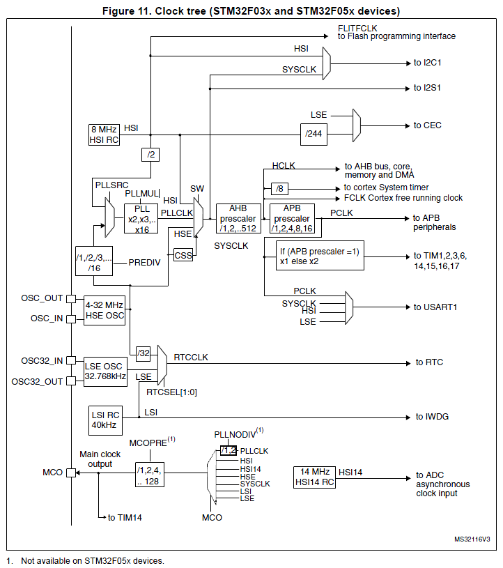 Figure 9.1: STM32F0 clock tree showing where timer clocks are derived from [1]
The timer does not always count directly at the raw system clock. The incoming timer clock passes through a prescaler before it reaches the counter.
Timer Architecture
Start with the time-base unit used by the basic timers. The block diagram below shows the main building blocks of a timer configured as a pure counter.
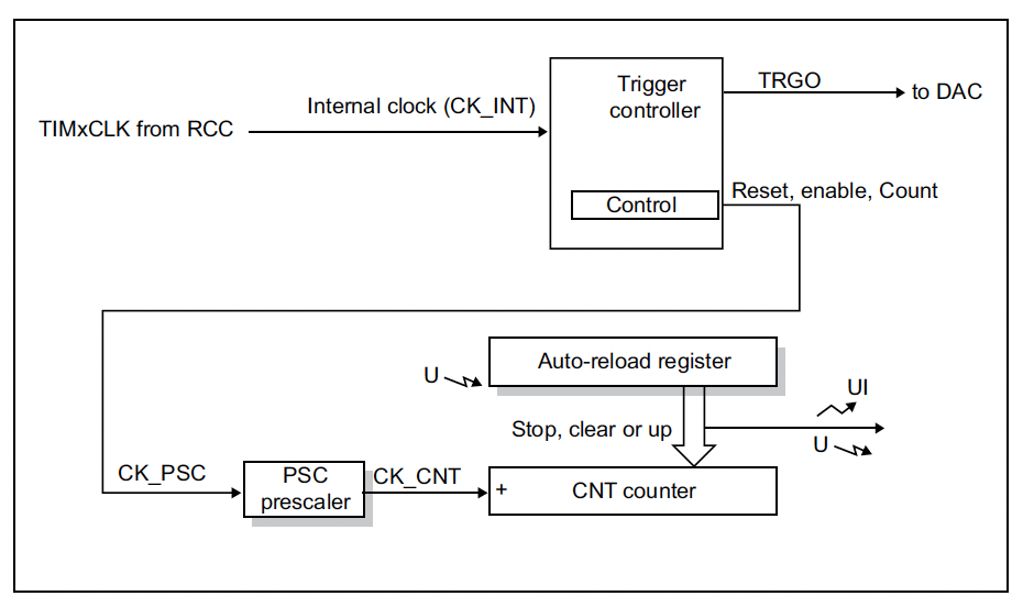 Figure 9.2: Basic timer architecture [1]
The timer registers used most often for time-base operation are:
-
TIMx_PSC: prescaler register -
TIMx_CNT: current counter value -
TIMx_ARR: auto-reload register -
TIMx_CR1: control register -
TIMx_DIER: interrupt enable register -
TIMx_SR: status register
The timer clock enters the prescaler first. The prescaler divides the incoming timer clock so that the counter runs more slowly than the APB timer clock. The divided clock, called CK_CNT, advances the counter register TIMx_CNT.
In the simplest up-counting mode, CNT starts at 0, increments by 1 on each CK_CNT pulse, and continues until it reaches the auto-reload value stored in ARR. At that point an update event occurs, the counter wraps back to 0, and the cycle repeats.
The Time-Base Unit
Two equations are fundamental when configuring timers:
$$f_{CNT} = \frac{f_{TIM}}{TIMx_ {PSC} + 1}$$
and
$$T_{update} = \frac{TIMx_ {ARR} + 1}{f_{CNT}} = \frac{(TIMx_ {PSC} + 1)(TIMx_ {ARR} + 1)}{f_{TIM}}$$
Where:
- $f_{TIM}$ is the timer input clock
- $f_{CNT}$ is the rate at which the counter increments
- $T_{update}$ is the time between update events
The +1 terms matter. A prescaler value of 0 means divide by 1, not divide by 0. Likewise, if ARR = 999, the timer counts 1000 steps: 0 through 999.
Worked Timing Example
Suppose the timer clock is 48 MHz (this is not the default value by the way, but it is possible to configure it to this frequency), the prescaler is 47, and the auto-reload value is 999.
$$f_{CNT} = \frac{48\,000\,000}{47 + 1} = 1\,000\,000 \text{ Hz}$$
So the counter advances once every microsecond. The update period is then:
$$T_{update} = \frac{999 + 1}{1\,000\,000} = 1 \text{ ms}$$
This setup creates a convenient 1 ms time base.
Update Events and Interrupts
When the counter reaches ARR, the timer raises an update event. The event can:
- reload the counter
- transfer preloaded values into active timer registers
- raise the
UIFflag inTIMx_SR - optionally request an interrupt if
UIEis enabled inTIMx_DIER
Start the timer by setting the CEN bit in TIMx_CR1. If update interrupts are required, then the UIE bit in TIMx_DIER must also be set, and the corresponding timer interrupt must be enabled in the NVIC.
For a simple polling approach:
while ((TIM3->SR & TIM_SR_UIF) == 0);
TIM3->SR &= ~TIM_SR_UIF;
For an interrupt-driven approach the timer must be clocked, configured, and started, and the NVIC must be enabled:
void TIM3_Init(void)
{
    RCC->APB1ENR |= RCC_APB1ENR_TIM3EN;  // Enable TIM3 clock

    TIM3->PSC = 47999;                    // 48 MHz / 48000 = 1 kHz
    TIM3->ARR = 999;                      // 1 kHz / 1000 = 1 Hz update rate
    TIM3->CNT = 0;                        // Clear counter

    TIM3->DIER |= TIM_DIER_UIE;           // Enable update interrupt
    NVIC_EnableIRQ(TIM3_IRQn);            // Enable TIM3 interrupt in NVIC

    TIM3->CR1 |= TIM_CR1_CEN;             // Start timer
}
and in the interrupt handler:
void TIM3_IRQHandler(void)
{
    if (TIM3->SR & TIM_SR_UIF)      //Check that the UIF flag is set
    {
        TIM3->SR &= ~TIM_SR_UIF;
        /* Do something every update event */
    }
}
Preload and Active Registers
When software writes to registers such as PSC, ARR, and the capture/compare registers, the value is often stored in a preload register first. The active value used by the timer hardware is only updated on an update event. This prevents timing glitches when values are changed while the timer is running.
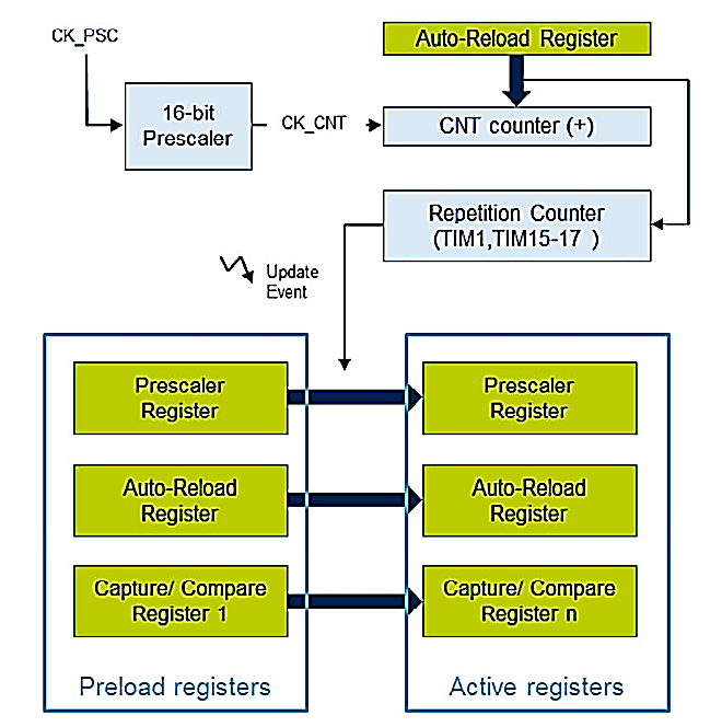 Figure 9.3: Preload and active timer registers [1]
This matters most in PWM applications (see below), where changing ARR or CCRx mid-period could create a malformed output pulse.
General-Purpose Timer Channels
General-purpose timers add capture/compare channels to the basic time-base unit. These channels can compare the running counter against reference values, drive output pins automatically, or copy the current counter value into a register when an external edge arrives.
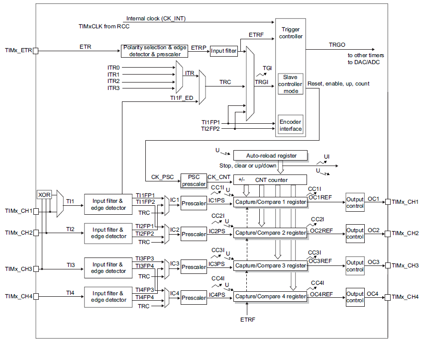 Figure 9.4: General-purpose timer structure [1]
The additional registers used most often are:
-
TIMx_CCR1toTIMx_CCR4: capture/compare registers -
TIMx_CCMR1andTIMx_CCMR2: capture/compare mode registers -
TIMx_CCER: capture/compare enable and polarity control
The same channel hardware can be used in either output compare mode or input capture mode. The CCxS bits in the CCMR register determine which role the channel performs. The pin(s) connected to each channel are listed in Tables 13-15 of the STM32F0 Datasheet - Note that this is not the Reference Manual! Pins are then configured to by used by the timer by setting the appropriate bits in the relevant GPIO port’s AFR (alternate function) register.
Output Compare
In output compare mode, the timer channel is configured as an output. The timer continuously compares the running counter value CNT against the compare register CCRx. When CNT == CCRx, an output compare event occurs.
The event:
- raises a
CCxIFflag - can set a channel output active (“active” can be chosen to mean a HIGH or a LOW value)
- can set it inactive (“inactive” is defined as the opposite state to “active”)
- can toggle it
- can optionally generate an interrupt
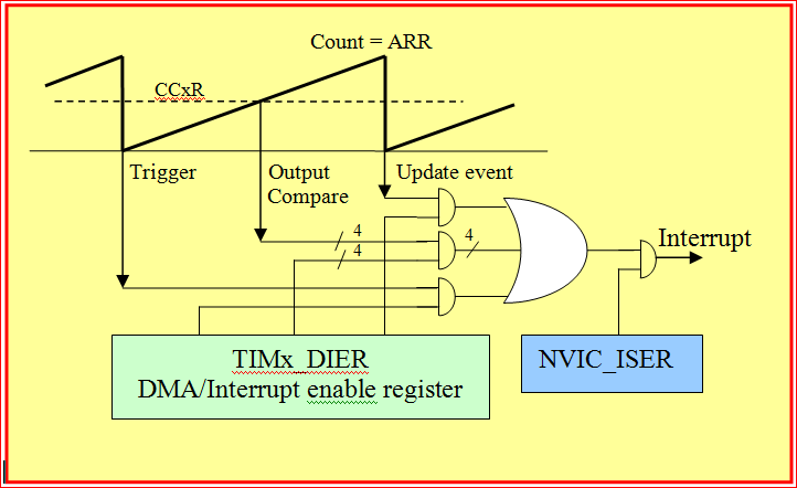 Figure 9.5: Output compare events can also generate interrupts [1]
In this course the most useful output compare modes are selected with the OCxM bits in the TIMx_CCMRx register:
-
001: set output active on compare match -
010: set output inactive on compare match -
011: toggle output on compare match -
110: PWM mode 1 -
111: PWM mode 2
The channel must also be enabled in TIMx_CCER using CCxE, and the pin must be configured for the correct alternate function on the GPIO peripheral.
Why Output Compare Is Useful
Use output compare when an action needs to happen at a specific counter value without CPU intervention:
- generate a pulse after a fixed delay
- toggle a pin at a regular interval
- generate interrupts tied to precise timer positions
Output Compare Configuration Sequence
A typical register-level output compare setup is:
- Enable the timer and GPIO clocks in
RCC. - Configure the chosen GPIO pin for alternate-function output.
- Set
TIMx_PSCandTIMx_ARRfor the desired output compare frequency. - Set
TIMx_CCRxfor the desired output compare position relative to the Update Event.
In TIMx_CCMR:
- Set
CCxS = 00so the channel is in output mode. - Set
OCxMto the desired output compare mode (i.e. set active, set inactive, toggle). - Enable compare preload using
OCxPEso duty cycle changes take effect cleanly on update events.
In TIMx_CCER:
- Choose the active level polarity with
CCxP. - Enable the channel with
CCxE.
In TIMx_DIER:
- Setup interrupts as needed (Timer Update Event, Output Compare Event, etc.)
In TIMx_CR1:
- Start the timer with
CEN.
Example Output Compare Register Setup
RCC->APB1ENR |= RCC_APB1ENR_TIM14EN;    // Enable TIM14 clock

// Depending on the pin chosen for use with the channel the
// GPIO port and pin must be configured for alternate function mode
// and the correct alternate function must be selected.
// For example, if PB1 is chosen for use with TIM14 channel 1:
// GPIOB->MODER |= GPIO_MODER_MODER1_1;    // Set PB1 to alternate function mode
// GPIOB->AFR[0] &= ~(0 << (4 * 1));        // Set PB1 to TIM14 alternate function 0

TIM14->PSC  = 7;                        // 8 MHz / 8 = 1 MHz counter clock
TIM14->ARR  = 99;                       // 1 MHz / 100 = 10 kHz PWM period
TIM14->CCR1 = 30;                       // Program the compare value

TIM14->CCMR1 &= ~TIM_CCMR1_CC1S;        // Channel 1 as output
TIM14->CCMR1 |= TIM_CCMR1_OC1PE;        // Enable CCR1 preload
TIM14->CCMR1 |= TIM_CCMR1_OC1M_0 | TIM_CCMR1_OC1M_1;       // Set output compare mode to Toggle

TIM14->CCER |= TIM_CCER_CC1E;           // Enable channel output
TIM14->CR1  |= TIM_CR1_CEN;             // Start timer
Pulse-Width Modulation (PWM)
PWM uses output compare to create a repeating digital waveform with a duty cycle controlled by software. It is an extension of output compare mode on the STM32 where the CCRx register is used to control a setting a pin level active (or inactive) at a specific point in the timer period, and then using the update event (i.e. the ARR register) to set that pin inactive (or active) at a different point in the timer period.
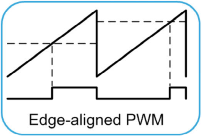 Figure 9.6: Edge-aligned PWM waveform [1]
In a standard edge-aligned PWM setup:
-
ARRsets the PWM period, and therefore the PWM frequency. Typically, the timer is configured here to raise its channel pin HIGH at the update event. I.e. opposite to the figure above. -
CCRxsets the point in the count at which the output changes state, and therefore the duty cycle. Typically, the timer is configured here to set its channel pin LOW at the compare event.
For up-counting PWM mode 1:
$$f_{PWM} = \frac{f_{TIM}}{(TIMx_PSC + 1)(TIMx_ARR + 1)}$$
and approximately:
$$\text{Duty cycle} = \frac{TIMx_CCR_x}{TIMx_ARR + 1} \times 100\%$$
If a timer runs with ARR = 999 and CCR1 = 250, the output is high for one quarter of the cycle and the duty cycle is approximately 25%.
PWM Configuration Sequence
A typical register-level PWM setup is:
- Enable the timer and GPIO clocks in
RCC. - Configure the chosen GPIO pin for alternate-function output.
- Set
TIMx_PSCandTIMx_ARRfor the desired PWM frequency. - Set
TIMx_CCRxfor the desired duty cycle.
In TIMx_CCMR:
- Set
CCxS = 00so the channel is in output mode. - Set
OCxMto PWM mode 1 or PWM mode 2. - Enable compare preload using
OCxPEso duty cycle changes take effect cleanly on update events.
In TIMx_CCER:
- Choose the active level polarity with
CCxP. - Enable the channel with
CCxE.
In TIMx_DIER:
- Setup interrupts as needed (Timer Update Event, Capture/Compare Event, etc.)
In TIMx_CR1:
- Start the timer with
CEN.
For example, if the timer clock is 48 MHz, then choosing PSC = 47 gives a 1 MHz counting rate. If ARR = 99, the PWM frequency becomes:
$$f_{PWM} = \frac{1\,000\,000}{100} = 10 \text{ kHz}$$
If CCR1 = 30, the duty cycle is approximately 30%.
Example PWM Register Setup
RCC->APB1ENR |= RCC_APB1ENR_TIM3EN;     // Enable TIM3 clock

// Depending on the pin chosen for use with the channel the
// GPIO port and pin must be configured for alternate function mode
// and the correct alternate function must be selected.
// For example, if PC6 is chosen for use with TIM3 channel 1:
// GPIOC->MODER |= GPIO_MODER_MODER6_1;    // Set PC6 to alternate function mode
// GPIOC->AFR[0] |= (0 << (4 * 6));         // Set PC6 to TIM3 alternate function 0

TIM3->PSC  = 47;                        // 48 MHz / 48 = 1 MHz counter clock
TIM3->ARR  = 99;                        // 1 MHz / 100 = 10 kHz PWM period
TIM3->CCR1 = 30;                        // 30% duty cycle

TIM3->CCMR1 &= ~TIM_CCMR1_CC1S;         // Channel 1 as output
TIM3->CCMR1 |= TIM_CCMR1_OC1PE;         // Enable CCR1 preload
TIM3->CCMR1 |= TIM_CCMR1_OC1M_1 | TIM_CCMR1_OC1M_2;  // PWM mode 1

TIM3->CCER |= TIM_CCER_CC1E;            // Enable channel output
TIM3->CR1  |= TIM_CR1_CEN;              // Start timer
The duty cycle can be changed at run time by writing a new value to CCR1.
Input Capture
Input capture uses the timer channel as an input. When an external edge arrives on the timer input pin, the timer copies the current counter value into CCRx.
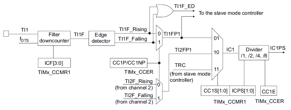 Figure 9.7: Input channel circuitry for timer capture [1]
Input capture can be used to measure:
- the period of a waveform
- pulse widths
- time of flight
- the time between external events
The timer hardware can also apply an input filter and select whether rising or falling edges cause a capture. A prescaler can be applied so that every second, fourth, or eighth valid edge is captured instead of every edge.
Input Capture Operation
In input capture mode:
- The counter runs continuously from the timer clock.
- An external edge arrives on the timer channel input.
- The current value of
CNTis copied into the channel’sCCRxregister. - The
CCxIFflag is set inTIMx_SR. - If enabled, a capture/compare interrupt is requested.
The timer acts as a stopwatch. If the counter runs at 1 MHz, each count is 1 µs, which keeps timing calculations simple.
Measuring Period with Two Captures
Assume a timer is configured so that:
f_CNT = 1 MHz- rising edges are captured on channel 2
If the first edge stores 12000 in CCR2 and the next edge stores 14500, then the elapsed time is:
$$\Delta counts = 14500 - 12000 = 2500$$
Since each count is 1 µs:
$$T = 2500 \text{ µs} = 2.5 \text{ ms}$$
and the input frequency is:
$$f = \frac{1}{2.5 \text{ ms}} = 400 \text{ Hz}$$
With a 16-bit timer, the counter may wrap around between captures. Calculate the difference modulo 65536 in that case.
Example Input Capture Setup
The following timer-side configuration sets up a rising-edge capture on channel 2:
TIM2->PSC = 47;                         // 1 MHz counter clock
TIM2->ARR = 0xFFFF;                     // Free-running 16-bit counter

TIM2->CCMR1 &= ~TIM_CCMR1_CC2S;
TIM2->CCMR1 |= TIM_CCMR1_CC2S_0;        // CC2 mapped as input on TI2

TIM2->CCER &= ~(TIM_CCER_CC2P | TIM_CCER_CC2NP);  // Rising edge
TIM2->CCER |= TIM_CCER_CC2E;            // Enable capture

TIM2->DIER |= TIM_DIER_CC2IE;           // Interrupt on capture
TIM2->CR1  |= TIM_CR1_CEN;              // Start timer
An interrupt handler can then read TIM2->CCR2 each time a capture occurs and subtract successive values to determine the period of the external signal.
Choosing Between Timer Modes
Think of the common timer modes in terms of the question they answer:
- Time base: “Has a fixed amount of time passed yet?”
- Output compare: “What should happen when the counter reaches this value?”
- PWM: “How can I generate a repeating waveform with a chosen duty cycle?”
- Input capture: “At what count value did this external event happen?”
These are not separate peripherals. They are different ways of using the same timer hardware.
Practical Notes for This Course
In this course timers are used for:
- generating PWM signals for motor control
- creating periodic interrupts
- timing external signals such as sensor pulses
Practical 6 uses timer-generated PWM, and later practicals build on that idea for motor drive and control. Match the timer configuration to the correct GPIO alternate function and channel for the pin chosen on the UCT board.
Summary
Timers are among the most important peripherals on the STM32 because they handle accurate timing without constant CPU involvement. The prescaler and auto-reload registers define the counting rate and overflow period. General-purpose timer channels extend this with output compare, PWM, and input capture. Once these ideas are understood, timers become a flexible tool for delays, interrupts, waveform generation, measurement, and closed-loop control.