Communication Interfaces
Table of Contents
- Communication Interfaces
- References
Microcontrollers rarely operate alone. They often need to exchange data with sensors, displays, motor drivers, other microcontrollers, and PCs. This chapter introduces the communication interfaces most commonly used in this course: UART/USART, I2C, and SPI.
The lecture slides used for this section are available here.
Introduction to Communication
In an embedded system, data is often collected in one place and used somewhere else. A sensor may measure a temperature, a microcontroller may process the reading, and a display or PC may show the result. The communication interface is the set of electrical signals, timing rules, and data framing rules that allows those devices to exchange information reliably.
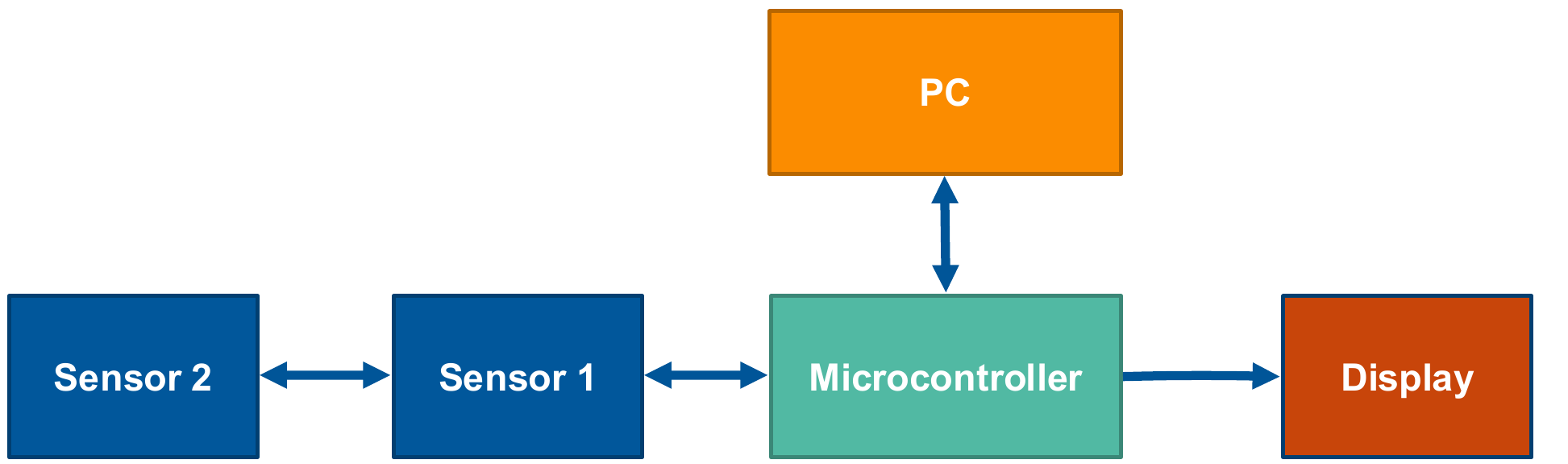 Figure 12.1: Microcontrollers often exchange data with sensors, displays, PCs, and other peripherals
At the highest level, digital communication can be either parallel or serial:
- Parallel communication sends multiple bits at the same time using multiple signal lines.
- Serial communication sends bits one after another using fewer signal lines.
Parallel communication can be fast over short distances, but it needs many pins and becomes awkward as systems grow. Serial communication is more common in small embedded systems because it uses fewer pins and is easier to route on a PCB. In this course we constrain ourselves to serial communication.
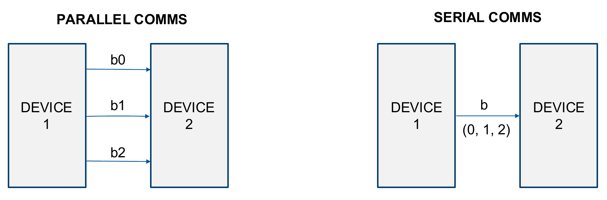 Figure 12.2: Parallel communication sends multiple bits at once, while serial communication sends bits sequentially
Serial Communication Concepts
Serial communication protocols differ in how they time the data transfer, how many devices can share the bus, and whether data can move in both directions at the same time.
Synchronous and Asynchronous Communication
In synchronous communication, the devices share a clock signal. The clock defines when the transmitter changes the data line and when the receiver samples it. SPI and I2C are synchronous protocols.
In asynchronous communication, there is no clock line. Both devices must be configured for the same bit timing before communication begins. UART is asynchronous, so both sides must agree on the baud rate, word length, parity, and stop-bit configuration.
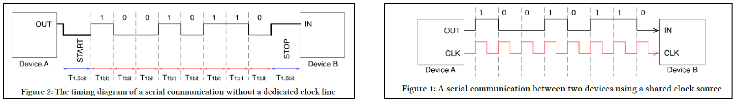 Figure 12.3: Synchronous communication uses a shared clock, while asynchronous communication relies on preconfigured bit timing [2]
| Type | Timing source | Typical protocols | Common signals |
|---|---|---|---|
| Synchronous | Shared clock line | SPI, I2C | Data plus clock |
| Asynchronous | Preconfigured bit period | UART | TX and RX |
Simplex, Half-Duplex, and Full-Duplex
The direction of communication also matters:
- Simplex: data moves in one direction only.
- Half-duplex: data can move in either direction, but not at the same time.
- Full-duplex: data can move in both directions at the same time.
UART is commonly used as a full-duplex point-to-point link with separate transmit and receive lines. I2C is a shared half-duplex bus. SPI is often full-duplex because data is shifted out and shifted in simultaneously.
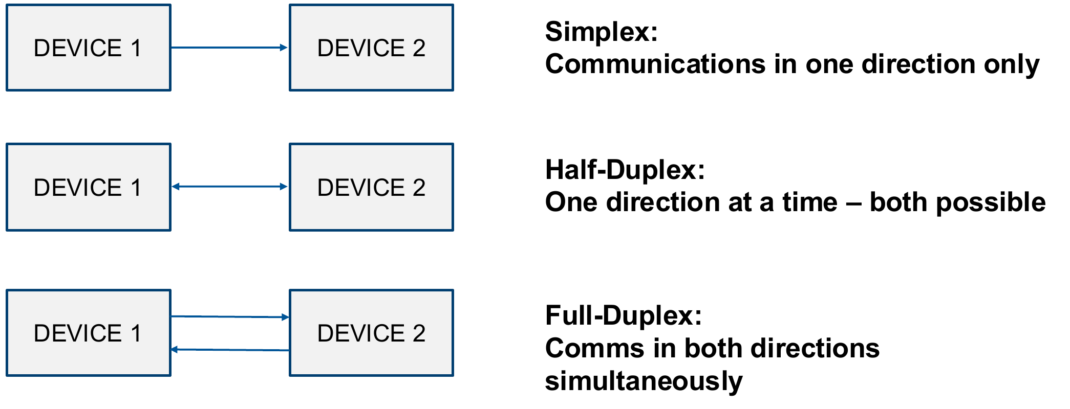 Figure 12.4: Simplex, half-duplex, and full-duplex communication directions
Packet Structure
Most communication protocols wrap the useful data in some form of packet or frame. A simple packet structure contains:
- A start condition or start symbol.
- The data field, usually grouped into bytes or words.
- Optional error checking, such as parity.
- A stop condition or stop symbol.
The exact meaning of the start and stop conditions depends on the protocol. In UART these are bit levels inside a frame. In I2C they are transitions on the SDA line while SCL is high.
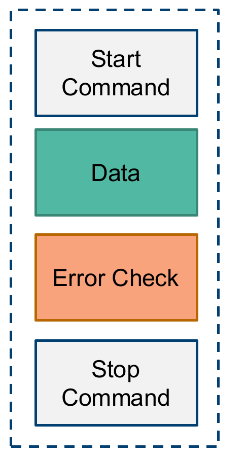 Figure 12.5: Simple packet structure containing a start command, data, optional error check, and stop command
UART and USART
UART stands for Universal Asynchronous Receiver Transmitter. Strictly speaking, UART is not a complete communication standard. It is the hardware block that serialises parallel data into bits for transmission and deserialises received bits back into data.
The STM32F0 implements USART peripherals, not only UART peripherals. USART stands for Universal Synchronous/Asynchronous Receiver Transmitter. The STM32 USART can be configured for asynchronous UART-style communication, synchronous communication, and some related modes such as SPI-like operation. In this course, the USART is mainly used in asynchronous mode.
UART Electrical Connection
A basic UART connection between two devices uses:
-
TX: transmit line -
RX: receive line -
GND: shared reference voltage
The TX pin of one device connects to the RX pin of the other. Both devices must share a ground reference.
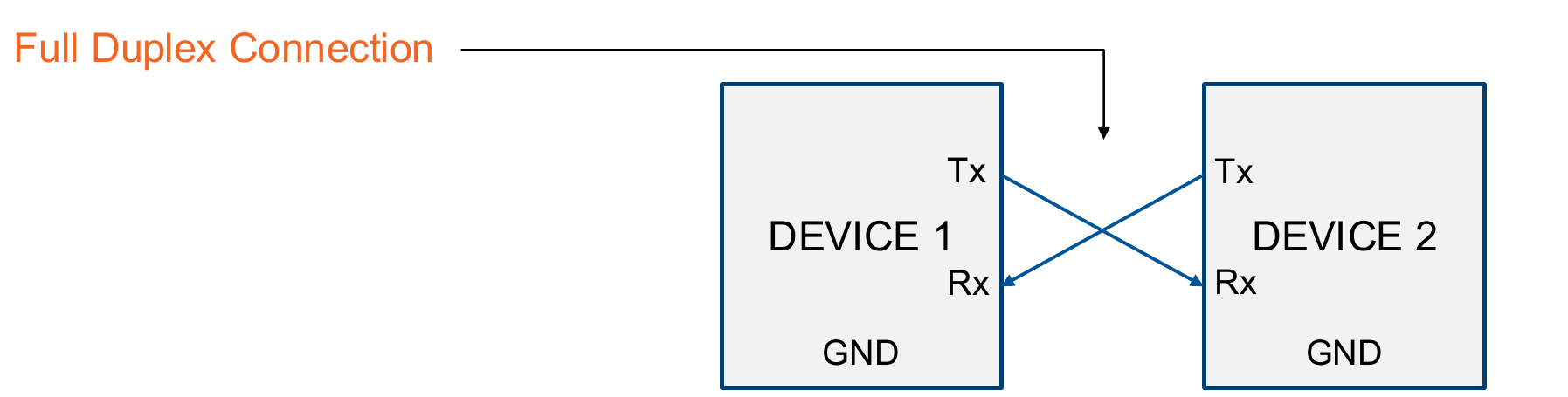 Figure 12.6: UART full-duplex connection using crossed transmit and receive lines with a shared ground
UART is normally used between two devices only. The idle state of the line is high, a start bit pulls the line low, the data bits follow, and the frame ends with one or more stop bits.
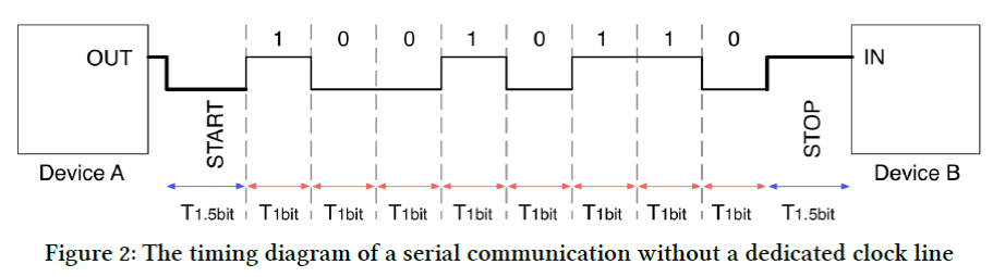 Figure 12.7: UART frame timing with an idle high line, start bit, data bits, and stop bit [2]
In the figure above, note that the START and STOP bits have a period of 1.5 $T_{1bit}$. This period is usally configurable by the hardware to various values: 1 bit, 1.5 bits or 2 bits. On the STM32F0, the START bit is always 1 bit in length, while the STOP bits are configurable.
Baud Rate
The baud rate defines the number of bit periods per second. Common baud rates include:
-
9600bit/s -
19200bit/s -
115200bit/s
Both devices must use the same baud rate. If the transmitter and receiver are configured for different rates, the receiver will sample bits at the wrong times and the received data will be unreliable.
On the STM32F0, the USART baud-rate register is configured from the peripheral clock:
$$\text{USART_BRR} = \frac{f_{CK}}{\text{baud}}$$
For example, with a 48 MHz USART clock and a baud rate of 115200 bit/s:
$$\text{USART_BRR} = \frac{48\,000\,000}{115\,200} \approx 417$$
which is 0x1A1 in hexadecimal.
UART Frame Format and Parity
A typical UART frame contains:
- An idle high state before transmission.
- A start bit.
- Data bits.
- Optional parity bit.
- One or more stop bits.
Parity is a simple error check. An extra bit is added so that the total number of 1 bits is either even or odd:
-
Even parity: data bits plus parity bit contain an even number of
1s. -
Odd parity: data bits plus parity bit contain an odd number of
1s.
 Figure 12.8: UART packet structure when an error-checking parity field is included
Parity can detect some single-bit errors, but it is not a complete data integrity mechanism.
RS-232
RS-232 is an asynchronous serial communication interface standard that commonly uses UART data framing, but not STM32 logic-level voltages. The STM32 USART pins use logic levels around 0 V and 3.3 V. RS-232 uses larger inverted voltage levels:
- Logic high: approximately
-3 Vto-15 V - Logic low: approximately
+3 Vto+15 V
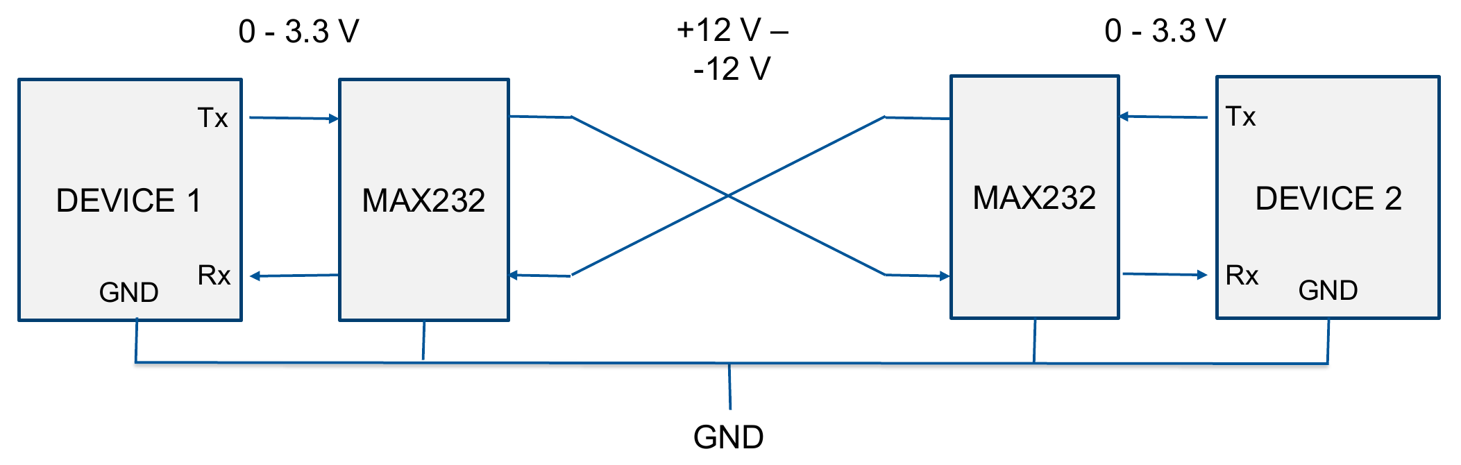 Figure 12.9: RS-232 communication requires line drivers to translate between logic-level UART signals and larger RS-232 voltage swings
Because of this voltage difference, an STM32 cannot connect directly to an RS-232 signal. A line-driver IC is required to translate between STM32 logic levels and RS-232 voltage levels. An example of this is the MAX232 which can be added to the UCT development board as shown below.
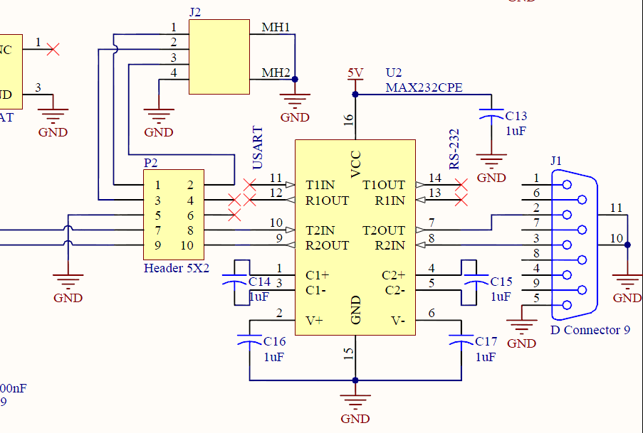 Figure 12.10: MAX232 level-shifting circuit used to connect STM32 USART pins to an RS-232 connector
flowchart LR
    MCU[STM32 USART pins] --> L1[MAX232]
    L1 --> DB9[RS-232 connector]
    DB9 --> L2[MAX232]
    L2 --> DEV[Other UART device]
RS-232 can work over longer distances than direct logic-level UART because it uses a larger voltage swing. For short connections between two STM32 boards, direct UART-to-UART communication is possible if both boards use compatible logic levels and share a ground.
USART on the STM32F0
The STM32F051 has two USART peripherals:
-
USART1, clocked fromAPB2 -
USART2, clocked fromAPB1
The transmit and receive pins must be configured as alternate-function GPIO pins before the USART can use them. On the course development board, USART1 can be used on PA9 and PA10, with alternate function AF1.
The USART registers used most often are:
-
USARTx_CR1: control register 1, including USART enable, transmitter enable, receiver enable, parity, word length, and interrupt enables. -
USARTx_CR2: control register 2, including stop-bit configuration. -
USARTx_BRR: baud-rate register. -
USARTx_ISR: interrupt and status register. -
USARTx_TDR: transmit data register. -
USARTx_RDR: receive data register.
In the figure below, if only the top two lines are connected, the USART peripheral is in UART mode, while the addition of the clock line facilitate USART.
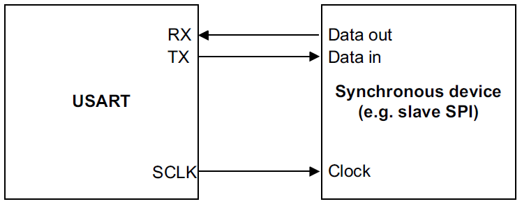 Figure 12.11: USART hardware can support synchronous operation as well as asynchronous UART-style communication [1]
Figure 12.12 below shows the bloack diagram of the USART data and logic control path on the STM32F0.
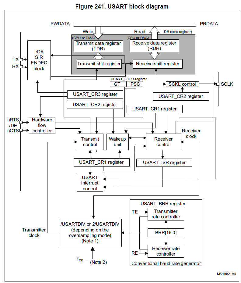 Figure 12.12: STM32F0 USART data path and control logic [1]
USART Control Register 1
The USART_CR1 register is the primary configuration register for the USART peripheral. It controls the core operating parameters including:
-
Word length: set via the
Mbits to configure 7, 8, or 9 data bits per frame. -
Transmit and receive enables: the
TEandREbits enable the transmitter and receiver respectively. -
Parity selection: the
PCEbit enables parity checking, and thePSbit selects even or odd parity. -
Interrupt enables: various bits in
CR1enable interrupts for transmit, receive, and error events (see the status flags below). -
USART enable: the
UEbit must be set to activate the peripheral.
Additional control registers configure complementary features.
USART Status Flags
The USART_ISR register contains flags that describe the state of the peripheral:
-
RXNE: receive data register not empty. A byte has arrived and can be read fromRDR. -
TXE: transmit data register empty. Software may write the next byte toTDR. -
TC: transmission complete. The last byte has fully left the transmitter. -
PE: parity error.
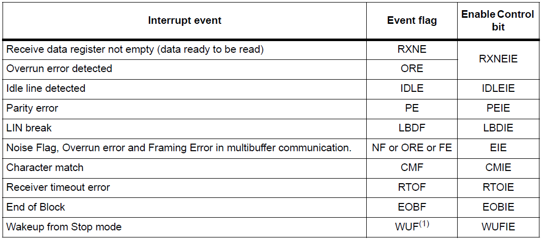 Figure 12.13: Example USART interrupt events and the corresponding enable bits [1]
When using interrupts, the interrupt handler should check the relevant flag before servicing the event, especially if more than one USART interrupt source has been enabled.
Transmit Data Register
The USART_TDR register holds the next byte to be transmitted. Software writes data into TDR, and the peripheral moves it into the internal transmit shift register when that register becomes free.
- The
TXEflag is raised when data has moved fromTDRinto the shift register, indicating thatTDRis ready for the next write. Writing new data toTDRclears theTXEflag. - The
TCflag is set once no new data has been written toTDRandTXEis high, meaning the last byte has fully left the transmitter.
Receive Data Register
The USART_RDR register contains the last byte received from the serial line. After the receiver has shifted in a complete frame, the resulting data is transferred into RDR.
- The
RXNEflag is raised when data has arrived inRDRand is ready to be read by software. - Reading
RDRclears theRXNEflag.
Transmit Timing
The diagram below illustrates the relationship between the TXE and TC flags during a back-to-back transmission of three frames.
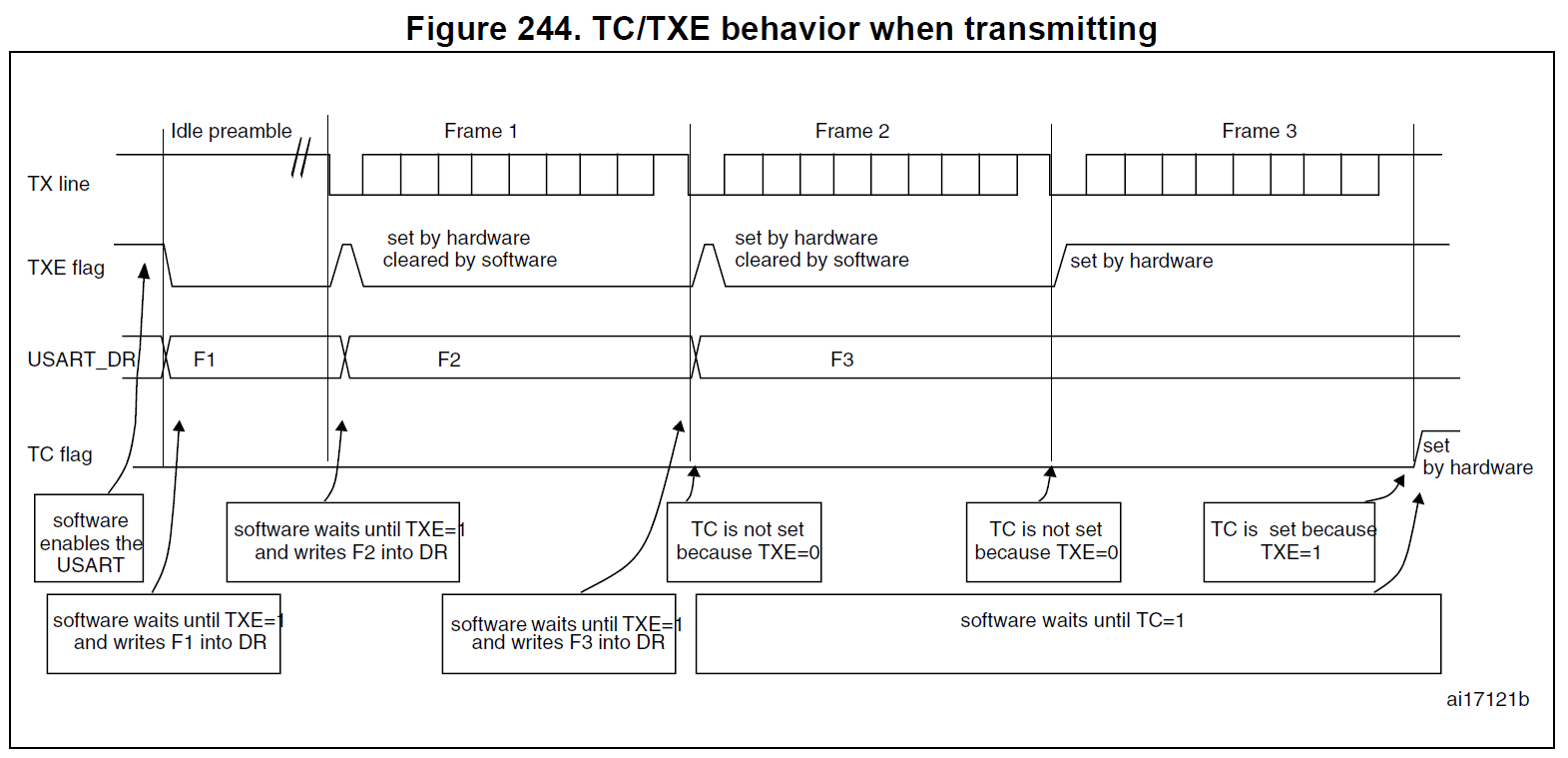 Figure 12.14: TC/TXE behaviour during back-to-back transmission [1]
After the USART is enabled, software waits for TXE to become high, then writes the first frame (F1) into TDR. This write clears TXE. While F1 is being shifted out on the TX line, TXE goes high again as soon as F1 moves from TDR into the shift register. Software can then write F2, which clears TXE once more. The same pattern repeats for F3.
The TC flag behaves differently. It remains low while there is still data to send (TXE was cleared by a recent write). Once the last frame (F3) has moved into the shift register and TXE is high again with no further writes, TC is set by hardware when the final stop bit has been transmitted. Software that needs to know when the entire stream has left the transmitter should wait for TC, whereas waiting for TXE is sufficient when preparing the next byte.
USART Configuration Sequence
A typical asynchronous USART setup is:
- Enable the GPIO clock in
RCC_AHBENR. - Configure the TX and RX pins for alternate-function mode in
GPIOx_MODER. - Select the correct alternate function in
GPIOx_AFR. - Enable the USART peripheral clock in
RCC_APB2ENRorRCC_APB1ENR. - Configure the baud rate in
USARTx_BRR. - Configure word length, parity, and stop bits in
USARTx_CR1andUSARTx_CR2. - Enable transmitter and/or receiver mode in
USARTx_CR1(TEandRE). - Enable USART interrupts in
USARTx_CR1and the NVIC if needed. - Enable the USART by setting
UEinUSARTx_CR1.
The following example configures USART1 on PA9 and PA10 for 9600 bit/s, receive interrupts, transmit mode, and receive mode:
void init_USART1(void)
{
    RCC->AHBENR |= RCC_AHBENR_GPIOAEN;       // Enable GPIOA clock

    GPIOA->MODER |= GPIO_MODER_MODER9_1
                 |  GPIO_MODER_MODER10_1;   // PA9, PA10 alternate function

    GPIOA->AFR[1] |= (1 << (4 * 1))          // PA9 is AFR[1] field 1
                  |  (1 << (4 * 2));         // PA10 is AFR[1] field 2

    RCC->APB2ENR |= RCC_APB2ENR_USART1EN;    // Enable USART1 clock

    USART1->BRR = 48000000 / 9600;           // Baud rate
    USART1->CR1 |= USART_CR1_RXNEIE;         // RXNE interrupt enable
    USART1->CR1 |= USART_CR1_TE | USART_CR1_RE;
    USART1->CR1 |= USART_CR1_UE;             // Enable USART

    NVIC_EnableIRQ(USART1_IRQn);
}
The USART must be disabled when configuring some frame settings, such as parity and word length. Check the reference manual before changing configuration bits while the peripheral is running.
Transmitting Data
To transmit one byte, wait until TXE is set, then write the byte to TDR:
void usart1_write_byte(uint8_t data)
{
    while ((USART1->ISR & USART_ISR_TXE) == 0);
    USART1->TDR = data;
}
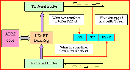 Figure 12.15: Functional view of the UART transmit and receive buffer mechanism
TXE means the transmit data register can accept another byte. TC means the final bit of the previous transmission has completed on the line.
Receiving Data with an Interrupt
The RXNE flag is raised when a received byte is available in RDR. Reading RDR clears RXNE.
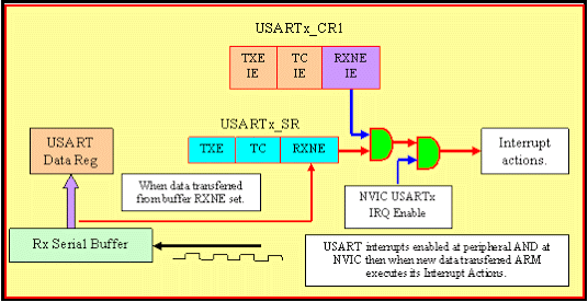 Figure 12.16: Functional view of a UART receive interrupt being generated from received data
The C code below shows an example of the ISR needed to read two bytes sent to the USART peripheral.
volatile uint8_t comm_data[2] = {0, 0};
volatile uint8_t counter = 0;

void USART1_IRQHandler(void)
{
    if (USART1->ISR & USART_ISR_RXNE)
    {
        comm_data[counter] = USART1->RDR;
        counter++;

        if (counter >= 2)
        {
            counter = 0;
        }
    }
}
SPI
SPI stands for Serial Peripheral Interface. It is a synchronous master-slave interface commonly used with displays, memory chips, ADCs, shift registers, and sensors.
SPI commonly uses four signals:
-
SCK: serial clock, generated by the master. -
MOSI: master out, slave in. -
MISO: master in, slave out. -
SSorNSS: slave select.
The master pulls a slave-select line low to choose the slave, then generates clock pulses. Data is shifted out and shifted in as the clock runs.
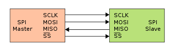 Figure 12.17: SPI master-slave connection showing clock, MOSI, MISO, and slave-select signals
When there are multiple slaves, the SCK, MOSI, and MISO lines are often shared, but each slave usually needs its own select line.
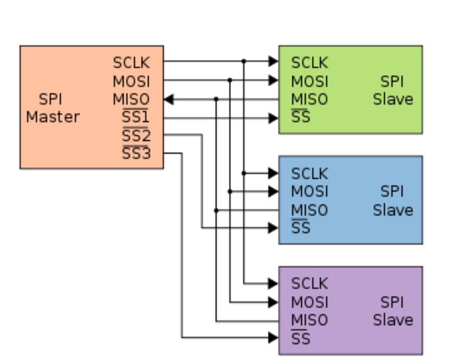 Figure 12.18: SPI can share clock and data lines across multiple slaves, but each slave usually needs its own select line
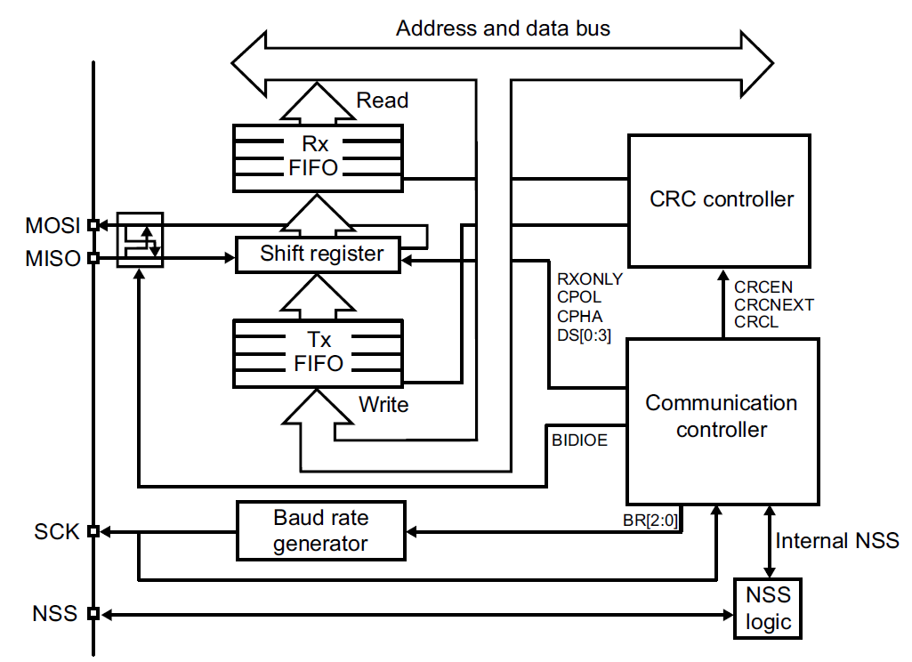 Figure 12.19: STM32F0 SPI block diagram [1]
Figure 12.19 shows the main data path inside the STM32F0 SPI peripheral. Software writes outgoing data to the SPI_DR data register. The SPI hardware then moves that data into an internal transmit buffer and shift register, where it is shifted out bit-by-bit on MOSI using the SCK clock. At the same time, incoming bits on MISO are shifted into a receive shift register and then made available to software through SPI_DR.
The transmit and receive paths include small FIFO buffers. FIFO stands for first in, first out: the first byte or word written into the buffer is the first one removed from it. A FIFO is useful because the CPU and the SPI pins do not operate at exactly the same instant. The CPU may write data in bursts, while the SPI peripheral sends it one bit at a time. Similarly, received data may arrive while the CPU is busy doing something else. The FIFO temporarily stores this data so that short delays in the firmware do not immediately stop the transfer or lose received bytes.
On the STM32 SPI peripheral, the status flags in the SPI Staus Register tell the firmware about the FIFO state. For example, TXE indicates that the transmit FIFO can accept more data, and RXNE indicates that the receive FIFO contains data that should be read. Good SPI code checks these flags before writing to or reading from SPI_DR.
SPI Modes and Clocking
SPI is synchronous, so the master controls the transfer speed through the serial clock. Two settings define the relationship between the clock and data:
-
CPOL: clock polarity, which sets the idle clock level. -
CPHA: clock phase, which chooses which clock edge captures data.
Both the master and slave must use compatible CPOL and CPHA settings. Otherwise, the receiver may sample data on the wrong edge.
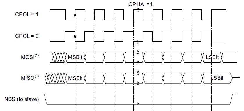 Figure 12.20: SPI timing relationship when
 CPHA = 0 [1]
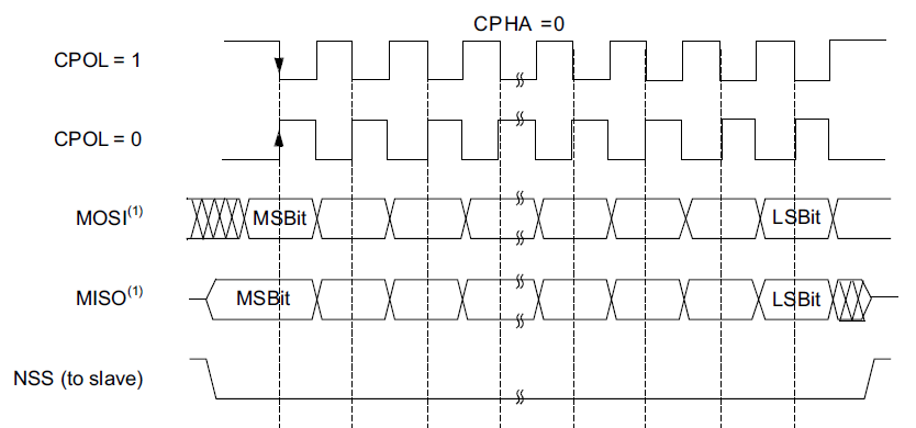 Figure 12.21: SPI timing relationship when
 CPHA = 1 [1]
Full-Duplex Transfers
SPI is naturally shift-register based. While the master shifts a bit out on MOSI, the slave can shift a bit back on MISO. This means that transmitting and receiving often happen at the same time.
This has an important consequence: to read from a slave, the master still has to transmit something so that clock pulses are generated. The transmitted byte may be dummy data, but it causes the slave’s response bits to be clocked into the master.
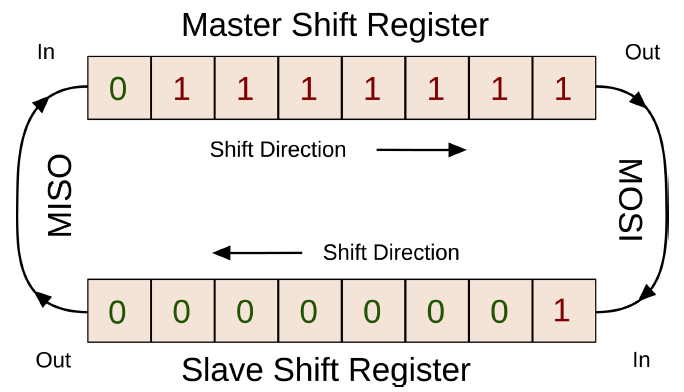 Figure 12.22: SPI full-duplex operation shifts data out and in at the same time
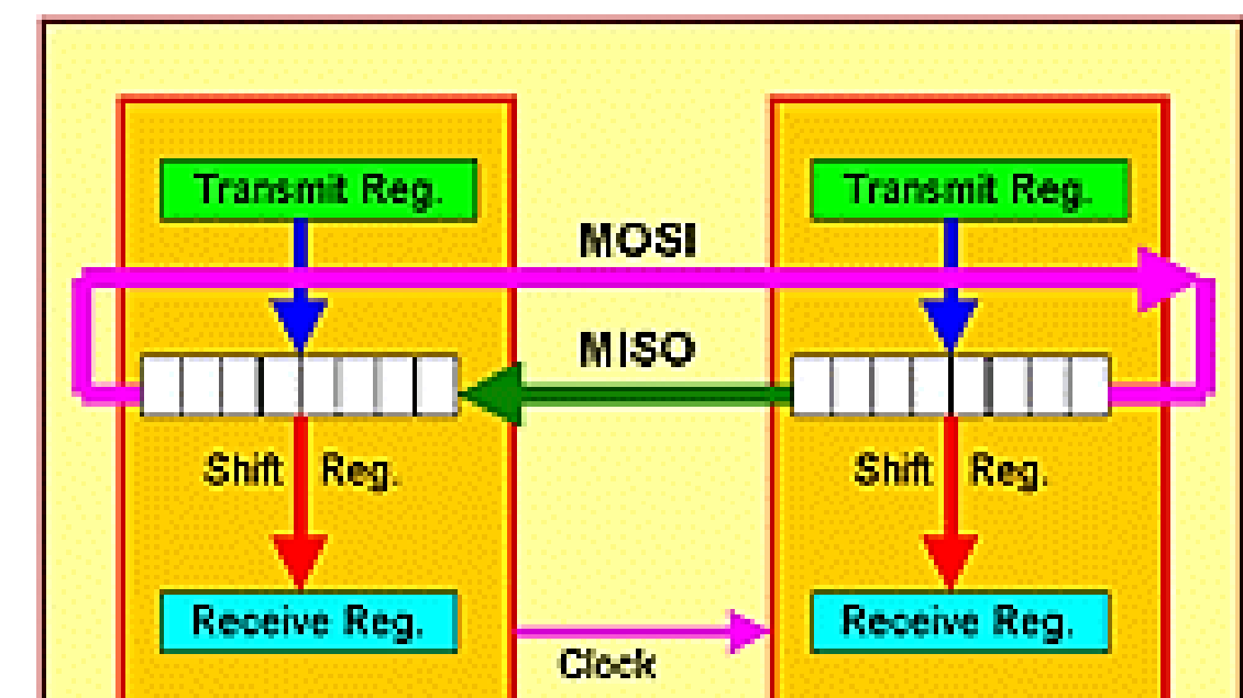 Figure 12.23: In full-duplex SPI, each clock pulse shifts data through the master and slave shift registers at the same time
SPI Strengths and Limitations
SPI has several advantages:
- It is usually faster than asynchronous serial communication.
- It has little protocol overhead.
- The receive hardware can be implemented as a simple shift register.
- It supports multiple slaves.
Its limitations are:
- It uses more signal lines than I2C.
- Each slave usually needs a separate select line.
- There is no built-in addressing or acknowledgement.
- The amount and meaning of data must be defined by the devices and firmware.
SPI on the STM32F0
The STM32F0 SPI registers used most often are:
-
SPI_CR1: baud-rate selection, clock polarity and phase, master mode, bidirectional mode, and SPI enable. -
SPI_CR2: data size, FIFO threshold, and slave-select output options. -
SPI_SR: status flags. -
SPI_DR: data register.
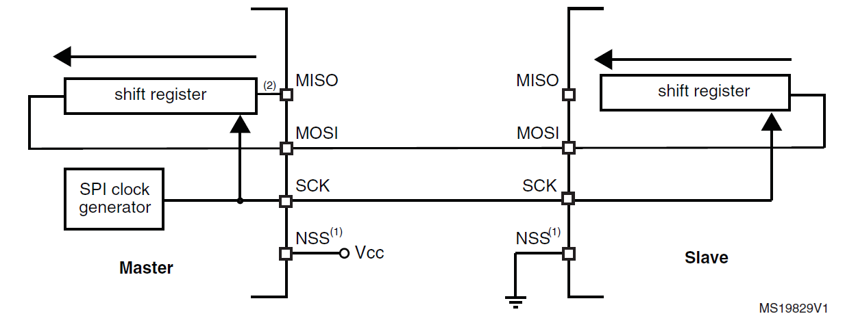 Figure 12.24: SPI simplex single-master, single-slave arrangement [1]
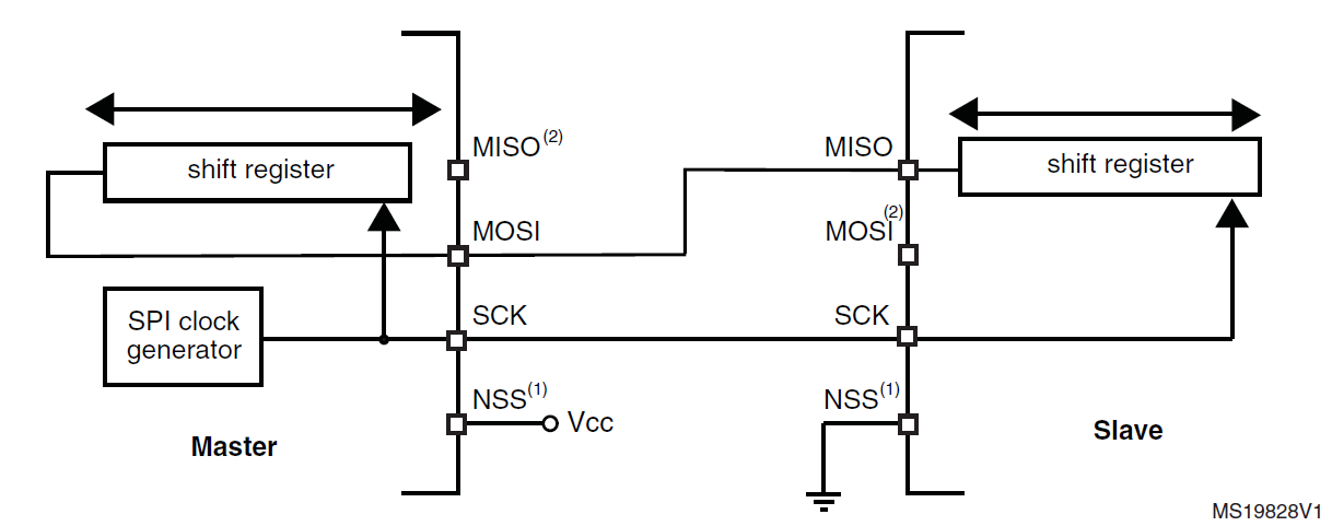 Figure 12.25: SPI half-duplex single-master, single-slave arrangement [1]
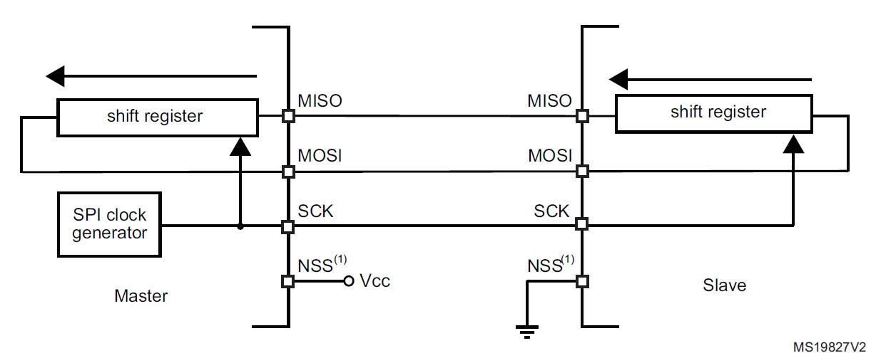 Figure 12.26: SPI full-duplex single-master, single-slave arrangement [1]
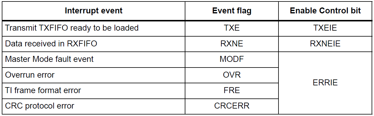 Figure 12.27: SPI interrupt events and enable bits [1]
The setup sequence for SPI is:
- Configure the GPIO pins for
SCK,MOSI,MISO, and slave select. - Enable the SPI peripheral clock.
- Configure the baud rate in
SPI_CR1. - Configure
CPOLandCPHA. - Select simplex, half-duplex, or full-duplex mode as needed.
- Configure master mode with
MSTR. - Configure the data size in
SPI_CR2. - Enable the SPI peripheral with
SPE.
SPI Configuration Example
The following example configures SPI2 using PB13 to PB15, with PB12 as a software-controlled slave-select pin.
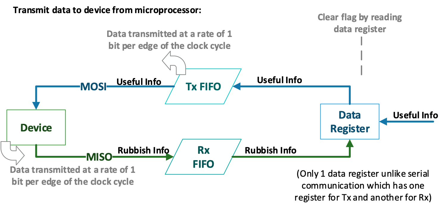 Figure 12.28: SPI control register 1 controls master mode, baud rate, clock configuration, and bidirectional settings [1]
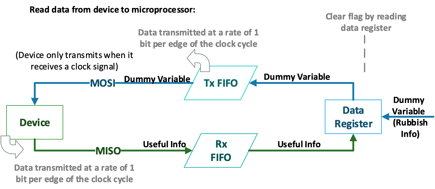 Figure 12.29: SPI control register 2 controls data size, FIFO threshold, and slave-select output behaviour [1]
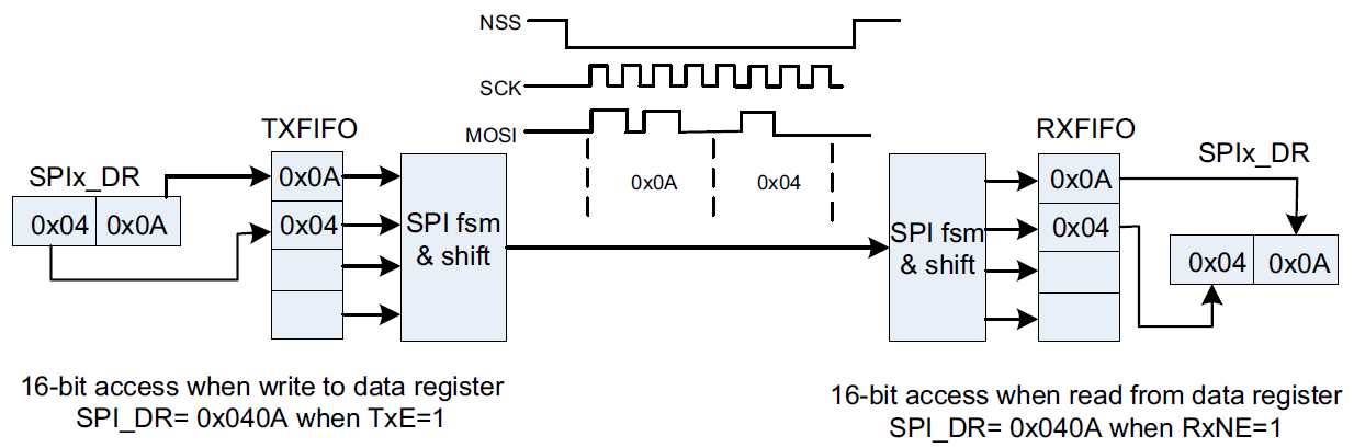 Figure 12.30: SPI status flags describe transmit and receive FIFO state [1]
void init_spi2(void)
{
    RCC->AHBENR |= RCC_AHBENR_GPIOBEN;       // Enable GPIOB clock

    GPIOB->MODER |= GPIO_MODER_MODER12_0     // PB12 output for SS
                 |  GPIO_MODER_MODER13_1     // PB13 SCK alternate function
                 |  GPIO_MODER_MODER14_1     // PB14 MISO alternate function
                 |  GPIO_MODER_MODER15_1;    // PB15 MOSI alternate function

    GPIOB->BSRR |= GPIO_BSRR_BS_12;          // Disable slave, SS high

    RCC->APB1ENR |= RCC_APB1ENR_SPI2EN;      // Enable SPI2 clock

    SPI2->CR1 |= SPI_CR1_BR_1 | SPI_CR1_BR_0; // fPCLK / 16
    SPI2->CR1 |= SPI_CR1_MSTR;               // Master mode

    SPI2->CR2 |= SPI_CR2_FRXTH               // 8-bit RX threshold
              |  SPI_CR2_DS_2
              |  SPI_CR2_DS_1
              |  SPI_CR2_DS_0;               // 8-bit data size

    SPI2->CR1 |= SPI_CR1_SPE;                // Enable SPI
}
SPI Write and Read Helpers
To write a byte, select the slave, write to SPI_DR, wait until a byte has been received, then read and discard the dummy receive data.
void spi2_write_byte(uint8_t data)
{
    GPIOB->BSRR |= GPIO_BSRR_BR_12;          // SS low

    SPI2->DR = data;

    while ((SPI2->SR & SPI_SR_RXNE) == 0);
    (void)SPI2->DR;                          // Discard dummy received byte

    GPIOB->BSRR |= GPIO_BSRR_BS_12;          // SS high
}
To read a byte, transmit dummy data so that the master generates clock pulses:
uint8_t spi2_read_byte(void)
{
    GPIOB->BSRR |= GPIO_BSRR_BR_12;          // SS low

    SPI2->DR = 0xFF;                         // Dummy byte to generate clocks

    while ((SPI2->SR & SPI_SR_RXNE) == 0);
    uint8_t received_data = SPI2->DR;

    GPIOB->BSRR |= GPIO_BSRR_BS_12;          // SS high

    return received_data;
}
I2C
I2C stands for Inter-Integrated Circuit. It is a synchronous two-wire bus used for communication between ICs on the same board or over short cable distances.
I2C uses two shared lines:
-
SCL: serial clock line -
SDA: serial data line
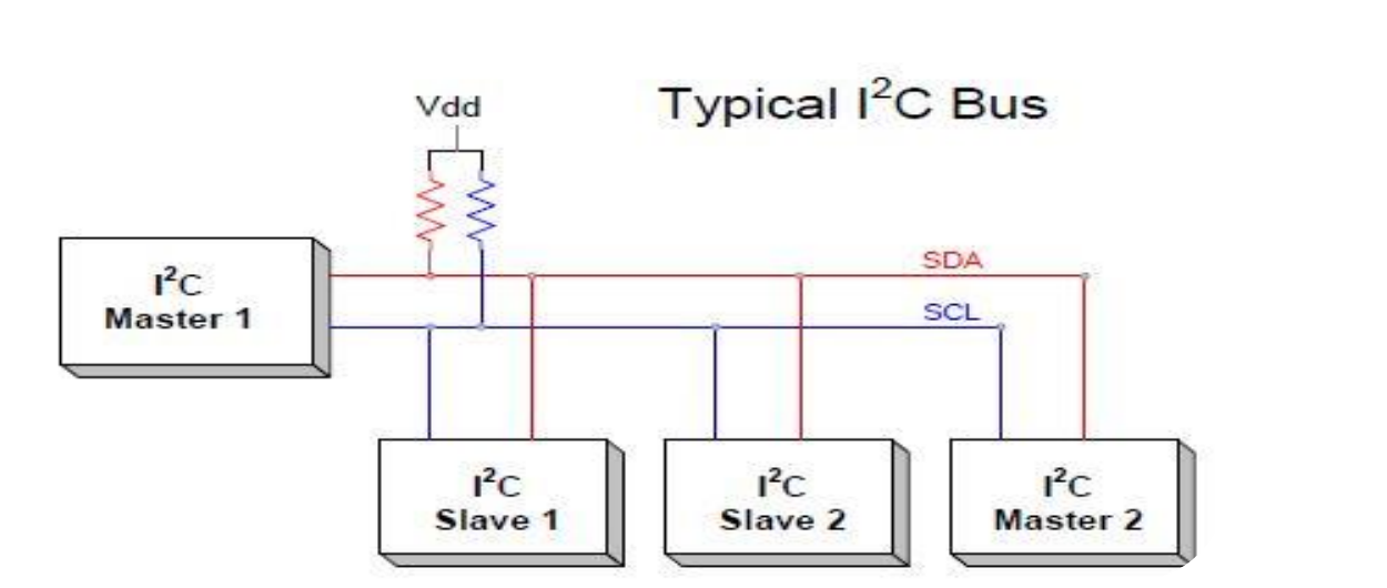 Figure 12.31: Typical I2C bus topology with shared SDA and SCL lines and pull-up resistors
Both lines are open-drain and require pull-up resistors. A device can pull the line low, but it does not actively drive the line high. The line returns high through the pull-up resistor when no device is pulling it low.
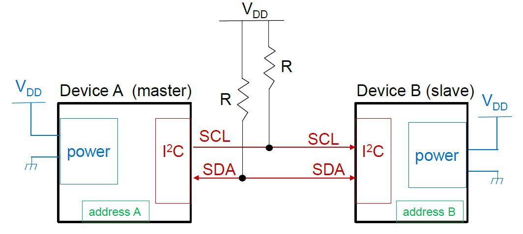 Figure 12.32: I2C hardware connection using open-drain SCL and SDA lines with pull-up resistors
flowchart LR
    M[Master] --- BUS[I2C bus: SCL and SDA]
    BUS --- S1[Slave 1]
    BUS --- S2[Slave 2]
    BUS --- S3[Slave 3]
I2C Bus Behaviour
I2C is a master-slave protocol. The master initiates communication and generates the clock. Each slave has an address, commonly a 7-bit address. The address frame is followed by a read/write bit:
-
0: write to the slave -
1: read from the slave
A basic I2C transaction contains:
- Start condition.
- Slave address.
- Read/write bit.
- Acknowledge bit.
- One or more data bytes.
- Acknowledge or not-acknowledge bits.
- Stop condition.
A start condition occurs when SDA falls while SCL is high. A stop condition occurs when SDA rises while SCL is high. During normal data transfer, SDA should only change while SCL is low.
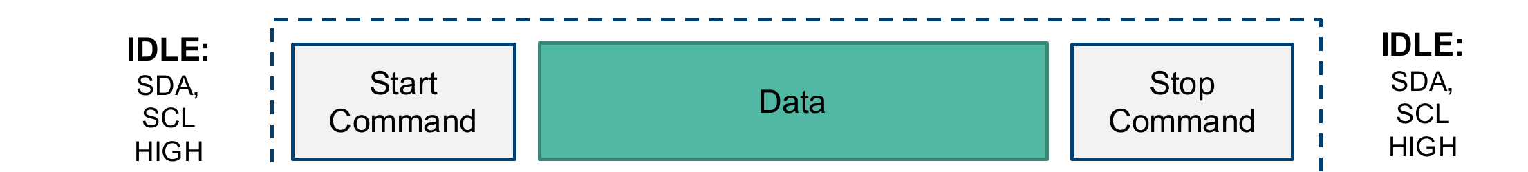 Figure 12.33: High-level I2C packet structure, showing idle bus state, start command, data, and stop command
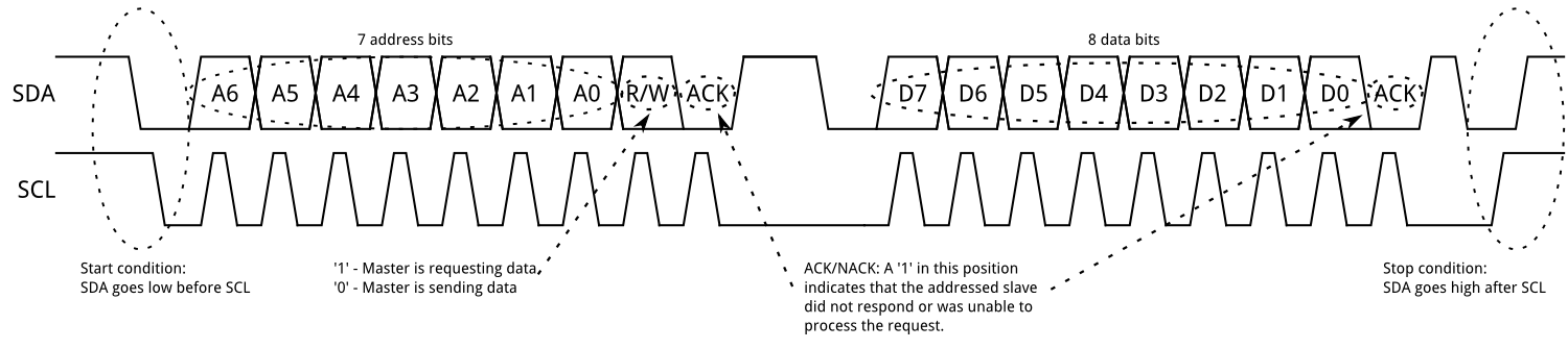 Figure 12.34: I2C address and data frame structure [4]
Repeated Start
Some devices require more than one message without releasing the bus. For example, a master may first write a register address to a sensor, then read data from that register. In this case, the master can issue a repeated start instead of a stop condition.
A repeated start is simply another start condition before the previous transaction has been ended with a stop condition. The master keeps control of the bus.
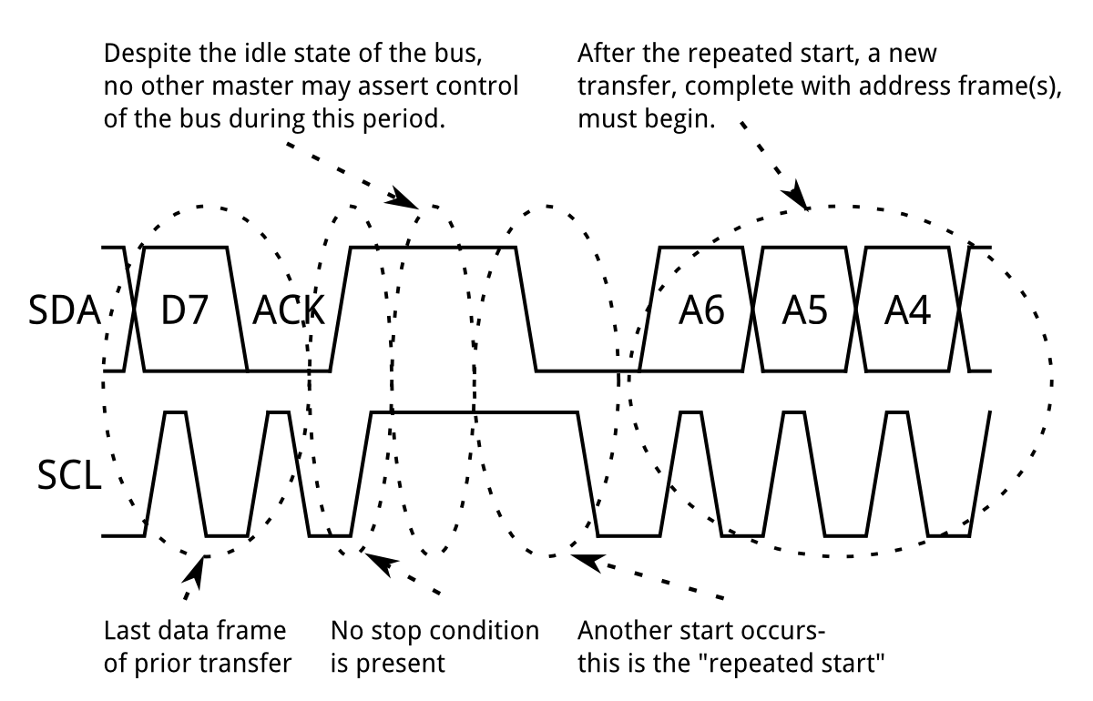 Figure 12.35: I2C repeated-start timing [4]
Clock Stretching
An I2C slave may hold SCL low to delay the master. This is called clock stretching. It is used when the slave is not ready for the next bit or byte. For example, a sensor may stretch the clock while waiting for an internal conversion to complete.
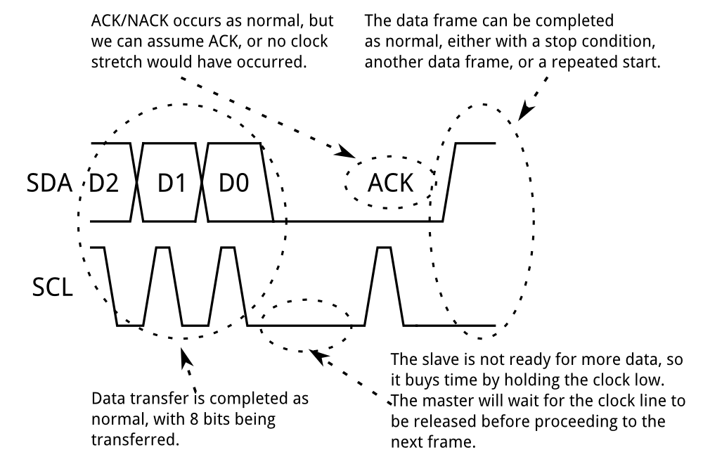 Figure 12.36: I2C clock stretching allows a slave to hold SCL low until it is ready [4]
I2C Strengths and Limitations
I2C is useful because many devices can share the same two wires, and devices are selected in software using addresses. It also includes acknowledgement bits, so the master can detect whether a slave responded.
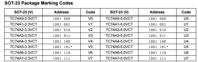 Figure 12.37: I2C multi-slave addressing example
The trade-offs are:
- It is intended for short distances.
- It is slower than SPI in most applications.
- The addressing and acknowledgement bits add overhead.
- A stuck-low bus line can prevent all bus communication.
Common I2C speeds include:
- Low speed:
10 kbit/s - Standard mode:
100 kbit/s - Fast mode:
400 kbit/s
I2C on the STM32F0
The STM32F0 includes two I2C peripherals. On the course board, useful pin mappings include:
-
I2C1onPB8andPB9 -
I2C2onPB10andPB11, orPF6andPF7
The I2C registers used most often are:
-
I2C_CR1: peripheral enable and interrupt enables. -
I2C_CR2: slave address, transfer direction, start and stop generation, and number of bytes. -
I2C_TIMINGR: timing configuration. -
I2C_ISR: status flags. -
I2C_RXDR: receive data register. -
I2C_TXDR: transmit data register.
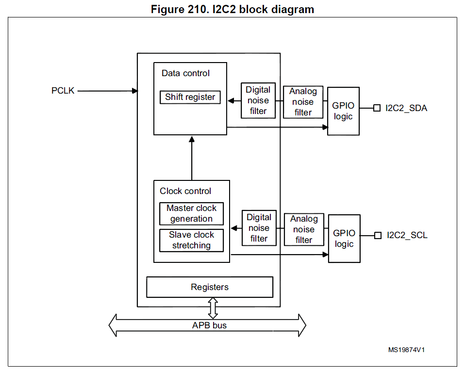 Figure 12.38: STM32F0 I2C peripheral feature overview [1]
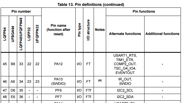 Figure 12.39: I2C pin mapping must be checked in the datasheet before choosing pins [3]
The timing register must be configured while the I2C peripheral is disabled.
I2C Configuration Example
The following example configures I2C2 on PF6 and PF7 for use as an I2C master. The timing values are representative values from the reference-manual style setup used in the lecture slides.
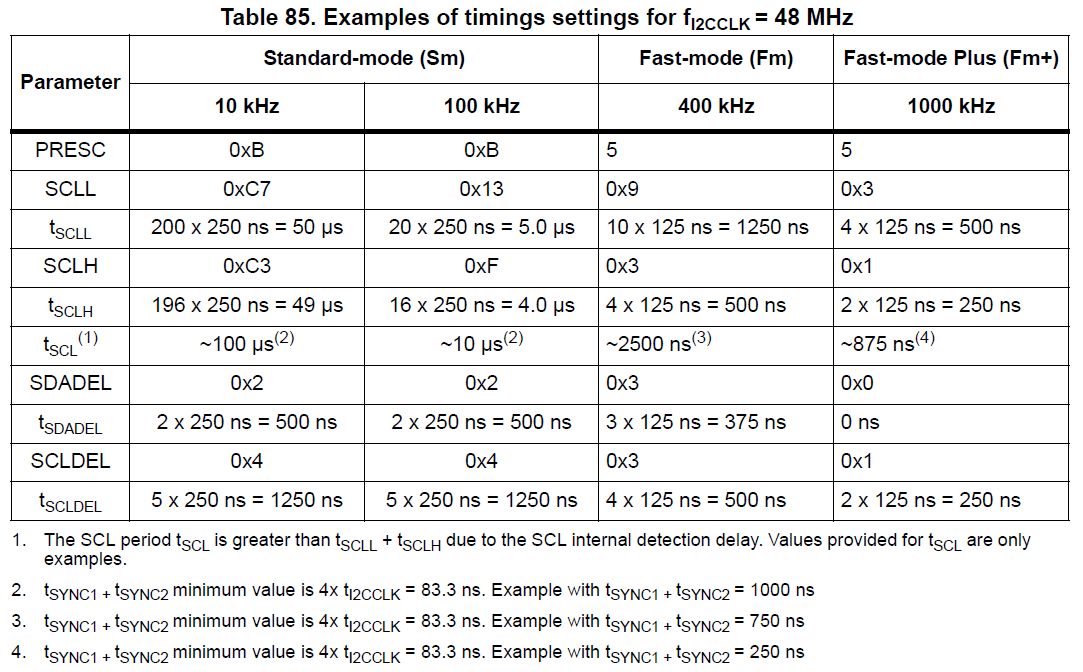 Figure 12.40: I2C timing configuration values can be taken from the reference manual or calculated from the timing equations [1]
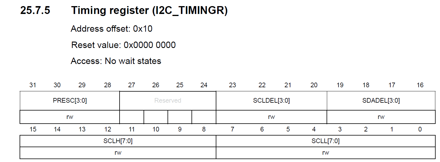 Figure 12.41: I2C timing register fields used to set SCL low time, SCL high time, data setup time, data hold time, and prescaler [1]
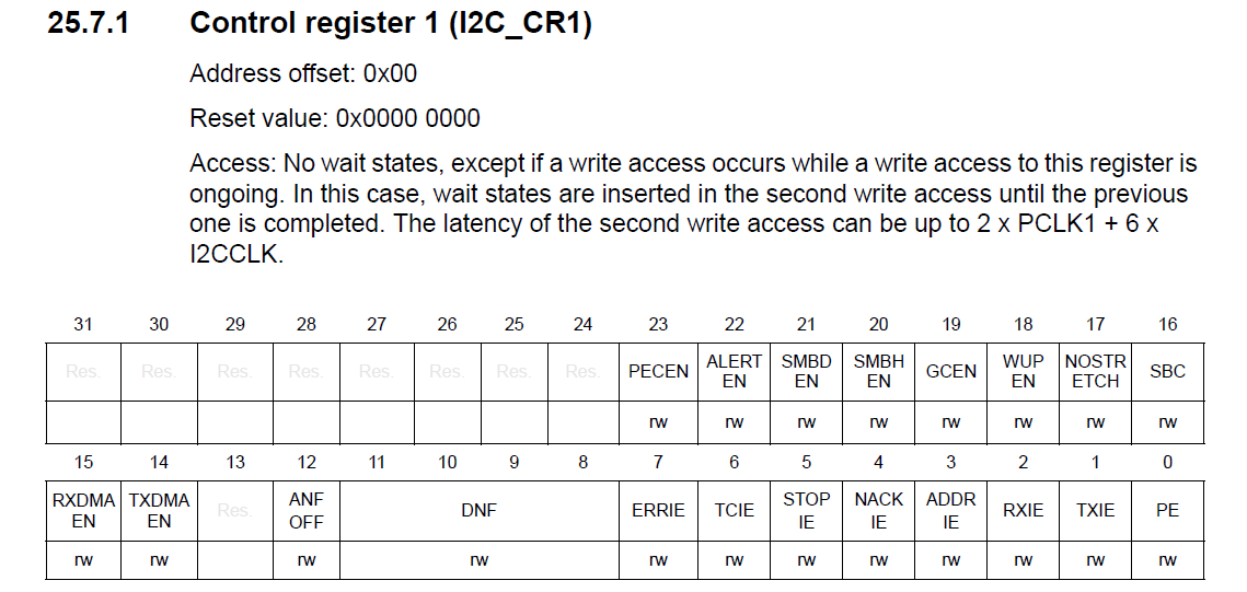 Figure 12.42: I2C control register 1 contains the peripheral enable and interrupt enable bits [1]
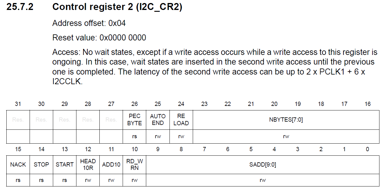 Figure 12.43: I2C control register 2 contains address, transfer direction, start, stop, and byte-count fields [1]
void init_i2c2(void)
{
    RCC->AHBENR |= RCC_AHBENR_GPIOFEN;       // Enable GPIOF clock

    GPIOF->MODER &= ~(GPIO_MODER_MODER6 | GPIO_MODER_MODER7);
    GPIOF->MODER |= GPIO_MODER_MODER6_1
                 |  GPIO_MODER_MODER7_1;    // Alternate function mode

    GPIOF->OTYPER |= GPIO_OTYPER_OT_6
                  |  GPIO_OTYPER_OT_7;      // Open-drain outputs

    RCC->APB1ENR |= RCC_APB1ENR_I2C2EN;      // Enable I2C2 clock

    I2C2->CR1 &= ~I2C_CR1_PE;                // Disable before timing setup

    I2C2->TIMINGR = (0xC7 << 0)              // SCLL
                  | (0xC3 << 8)              // SCLH
                  | (0x02 << 16)             // SDADEL
                  | (0x04 << 20)             // SCLDEL
                  | (0x0B << 28);            // PRESC

    I2C2->CR1 |= I2C_CR1_PE;                 // Enable I2C
}
I2C Read Example
The following code reads one byte from a TC74 temperature sensor. The TC74 has a 7-bit address of 0b1001000.
#define TC74ADDR 0b1001000

uint8_t tc74_read_temperature(void)
{
    I2C2->CR2 = 0;                           // Clear previous transfer setup
    I2C2->CR2 |= (TC74ADDR << 1);            // 7-bit address in SADD
    I2C2->CR2 |= (1 << 16);                  // NBYTES = 1
    I2C2->CR2 |= I2C_CR2_RD_WRN;             // Read transfer
    I2C2->CR2 |= I2C_CR2_START;              // Generate start

    while ((I2C2->ISR & I2C_ISR_RXNE) == 0);

    uint8_t temperature = I2C2->RXDR;

    I2C2->CR2 |= I2C_CR2_STOP;               // Generate stop

    return temperature;
}
In a robust application, the code should also check for acknowledgement failure and timeout conditions rather than waiting forever.
Choosing a Communication Interface
The best interface depends on the devices being connected and the constraints of the system.
| Interface | Wires | Timing | Typical use | Main advantage | Main limitation |
|---|---|---|---|---|---|
| UART/USART | TX, RX, GND | Asynchronous | PC links, simple device-to-device links | Simple point-to-point communication | Usually only two devices |
| I2C | SDA, SCL, GND | Synchronous | Sensors and ICs on one board | Many devices on two wires | Slower and short distance |
| SPI | SCK, MOSI, MISO, SS, GND | Synchronous | Displays, ADCs, memory, fast sensors | Fast and low overhead | More pins |
Use UART when two devices need a simple serial link, especially when connecting to a PC through USB-serial or RS-232 hardware. Use I2C when several low- to moderate-speed devices must share a small number of pins. Use SPI when speed and low overhead matter more than pin count.
Practical Notes for This Course
For communication practicals, always check four things before debugging the protocol itself:
- The peripheral clock is enabled in
RCC. - The GPIO pins are configured for the correct mode and alternate function.
- The electrical interface is correct, including shared ground, pull-up resistors for I2C, and level shifting for RS-232 if required.
- The STM32 settings match the external device settings or datasheet requirements.
Communication faults are often caused by pin configuration or electrical assumptions before they are caused by the protocol logic.
Summary
Serial communication allows the STM32 to exchange data with external devices using a small number of pins. UART/USART provides simple asynchronous point-to-point communication, with baud rate and frame format configured in advance. I2C provides a two-wire addressed bus for many short-distance devices. SPI provides fast synchronous transfers using a master clock and slave-select lines. Each interface has different trade-offs, so the correct choice depends on distance, speed, pin count, and the external devices being used.
References
[1] ST Microelectronics, “RM0091 Reference Manual”. May 2022. [Online]. Available: https://www.st.com/resource/en/reference_manual/rm0091-stm32f0x1stm32f0x2stm32f0x8-advanced-armbased-32bit-mcus-stmicroelectronics.pdf
[2] Carmine Noviello, “Mastering STM32”. Leanpub.
[3] SparkFun, “I2C”. [Online]. Available: https://learn.sparkfun.com/tutorials/i2c/all